


Quick Research
Generate reliable direction feasibility study reports for your R&D in just a few steps.

Technical Q&A
Discover and master advanced knowledge NOW. Basics, ideas, possibilities, all at once.

Find Solutions
As an expert in R&D theories, this can generate solutions to your technical problems instantly.

Evaluate Feasibility
Analyze your overall solution with one click, know your potential R&D risks in advance.

Monitor Landscape
Get weekly tech updates, stay abreast of the latest tech innovations and key insights.
Semiconductor substrate with islands of diamond and resulting devices
a technology of semiconductor substrate and diamond, which is applied in the direction of semiconductor devices, semiconductor/solid-state device details, electrical apparatus, etc., can solve the problems of corresponding increase in power consumption of semiconductor devices, placing greater demands on cooling solutions,
- Summary
- Abstract
- Description
- Claims
- Application Information
AI Technical Summary
Problems solved by technology
Method used
Image

Examples
Embodiment Construction
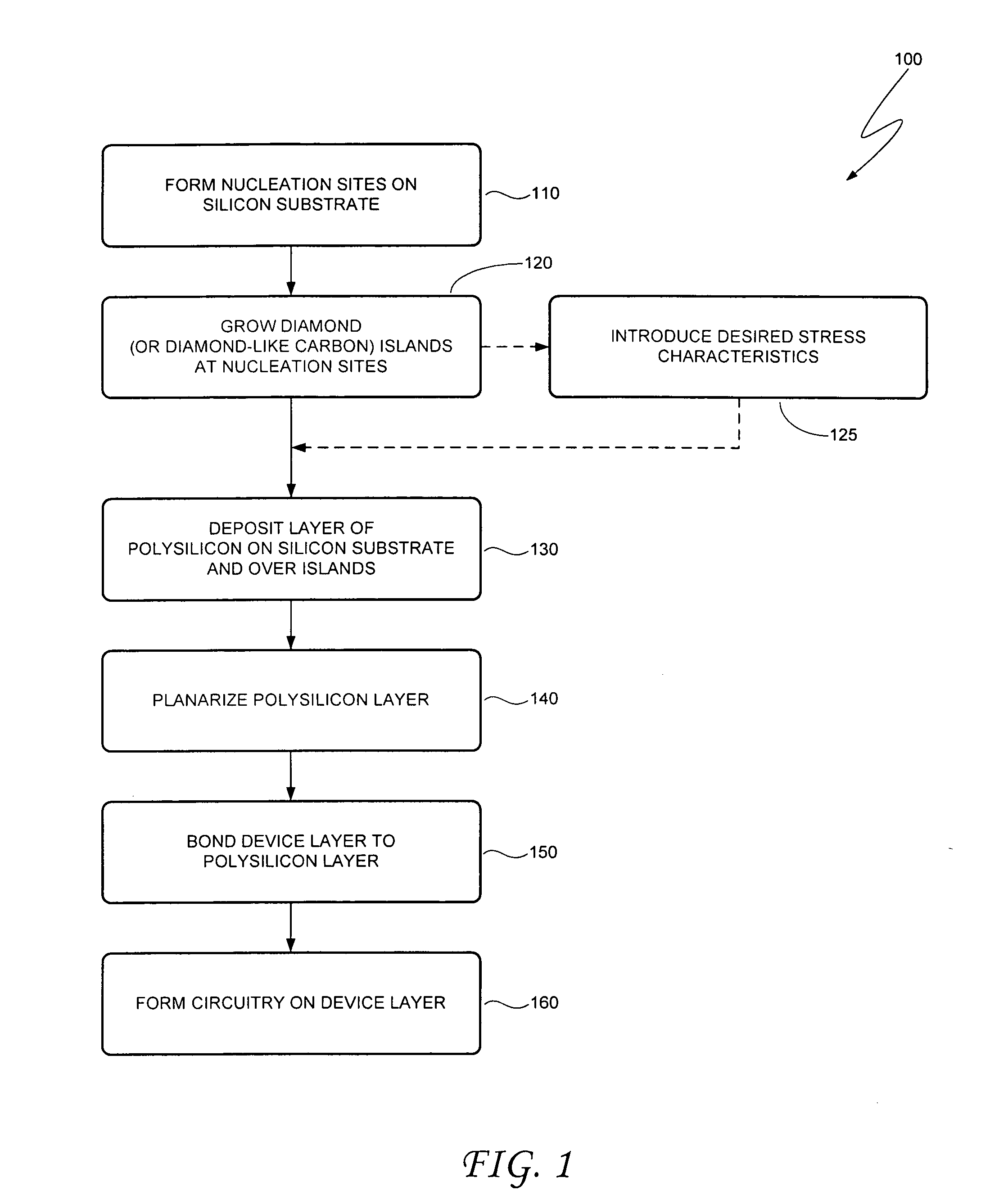
[0009] Turning now to FIG. 1, illustrated is an embodiment of a method 100 of fabricating a substrate having islands of diamond. Embodiments of the method 100 shown in FIG. 1 are further illustrated in the schematic diagrams of FIGS. 2A through 2F, and reference should be made to these figures as called out in the text below. Also, it should be noted that, although the embodiments are generally described below in the context of forming islands of diamond on a substrate, the disclosed embodiments are applicable to the formation of islands of other materials, such as diamond-like carbon.
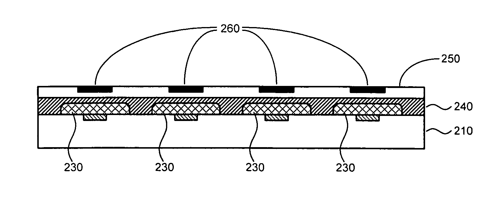
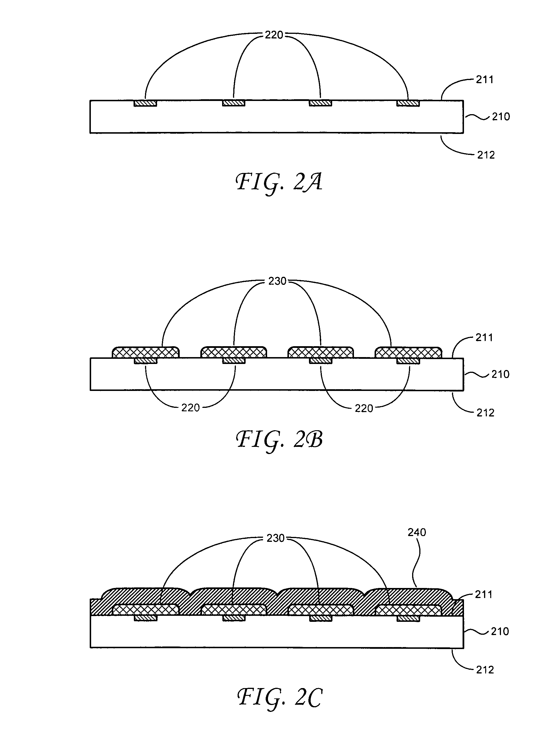
[0010] Referring to block 110 in FIG. 1, a number of nucleation sites are formed on a substrate comprised of silicon. This is illustrated in FIG. 2A, which shows a substrate 210. The substrate 210 may be viewed as having a first side 211 and an opposing second side 212. It should be understood, however, that the labels “first side” and “second side” are arbitrary and, further, that the various surface...
PUM
| Property | Measurement | Unit |
|---|---|---|
| tensile stresses | aaaaa | aaaaa |
| tensile stresses | aaaaa | aaaaa |
| thickness | aaaaa | aaaaa |
Abstract
Description
Claims
Application Information
 - R&D Engineer
- R&D Manager
- IP Professional
- Industry Leading Data Capabilities
- Powerful AI technology
- Patent DNA Extraction
Browse by: Latest US Patents, China's latest patents, Technical Efficacy Thesaurus, Application Domain, Technology Topic, Popular Technical Reports.
© 2024 PatSnap. All rights reserved.Legal|Privacy policy|Modern Slavery Act Transparency Statement|Sitemap|About US| Contact US: help@patsnap.com