
Tandem photovoltaic device and fabrication method thereof

Inactive Publication Date: 2007-03-29
SAMSUNG ELECTRONICS CO LTD
View PDF4 Cites 41 Cited by
  • Summary
  • Abstract
  • Description
  • Claims
  • Application Information

AI Technical Summary

Benefits of technology

[0015] Another aspect of the present invention includes a method for fabricating a tandem photovoltaic device by which the electric power generation costs of the photovoltaic device can be reduced and the power conversion efficiency of the photovoltaic device can be improved.

Problems solved by technology

However, silicon solar cells require the use of huge, expensive equipment and costly raw materials, incurring considerable fabrication costs.
In addition, silicon solar cells present numerous difficulties in improving the conversion efficiency of solar energy into electric energy.
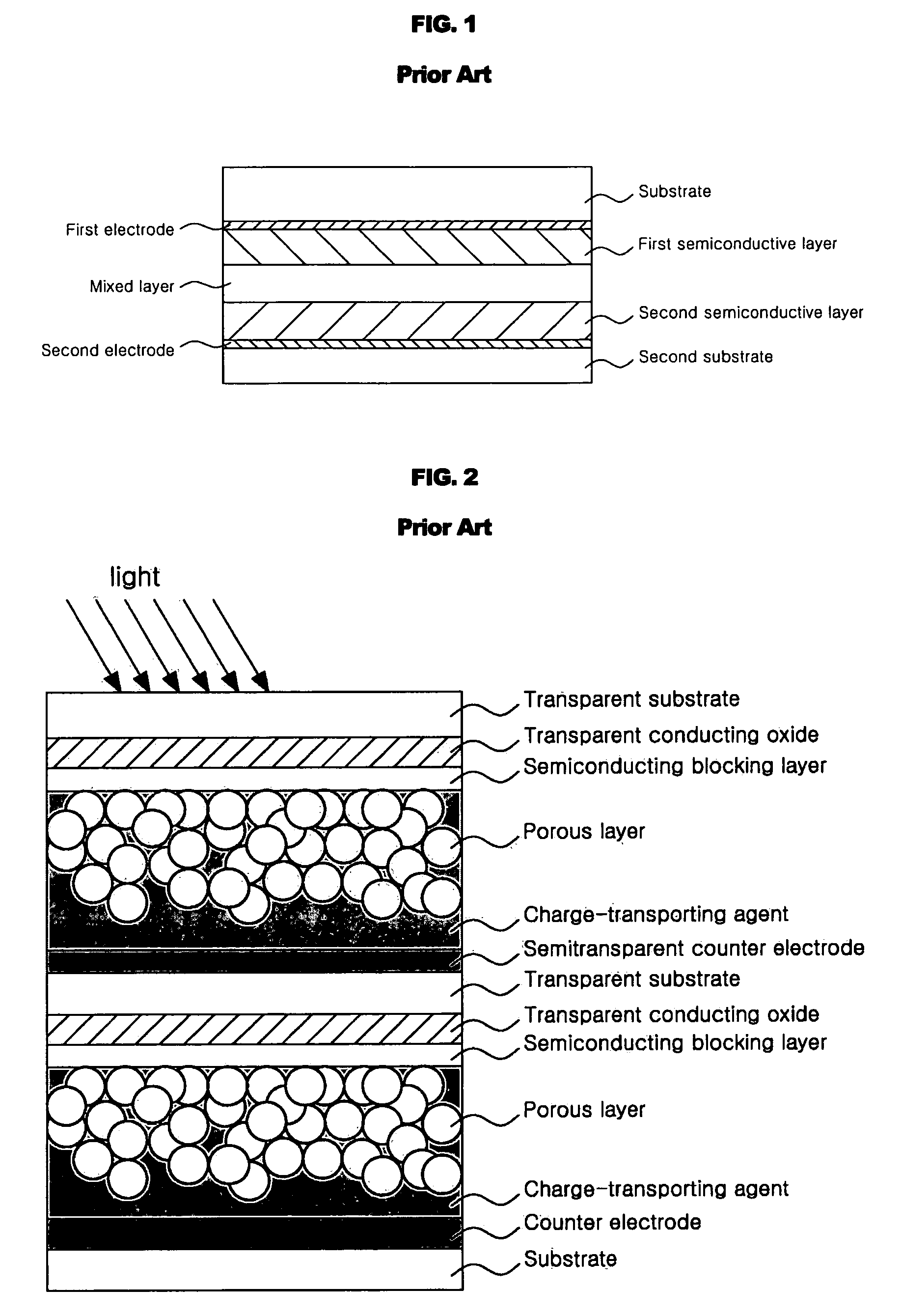
Accordingly, dye-sensitized solar cells are not suitable for use in a variety of portable electronic devices that are becoming gradually smaller in size and thickness.
In dye-sensitized solar cells, electric energy is generated when light is incident on a dye but the light absorbed by the dye is lost.
For these reasons, it has been believed that solar cells cannot be successfully fabricated into multilayer structures.

Method used


Image

  • Tandem photovoltaic device and fabrication method thereof
  • Tandem photovoltaic device and fabrication method thereof
  • Tandem photovoltaic device and fabrication method thereof

Examples


example 1

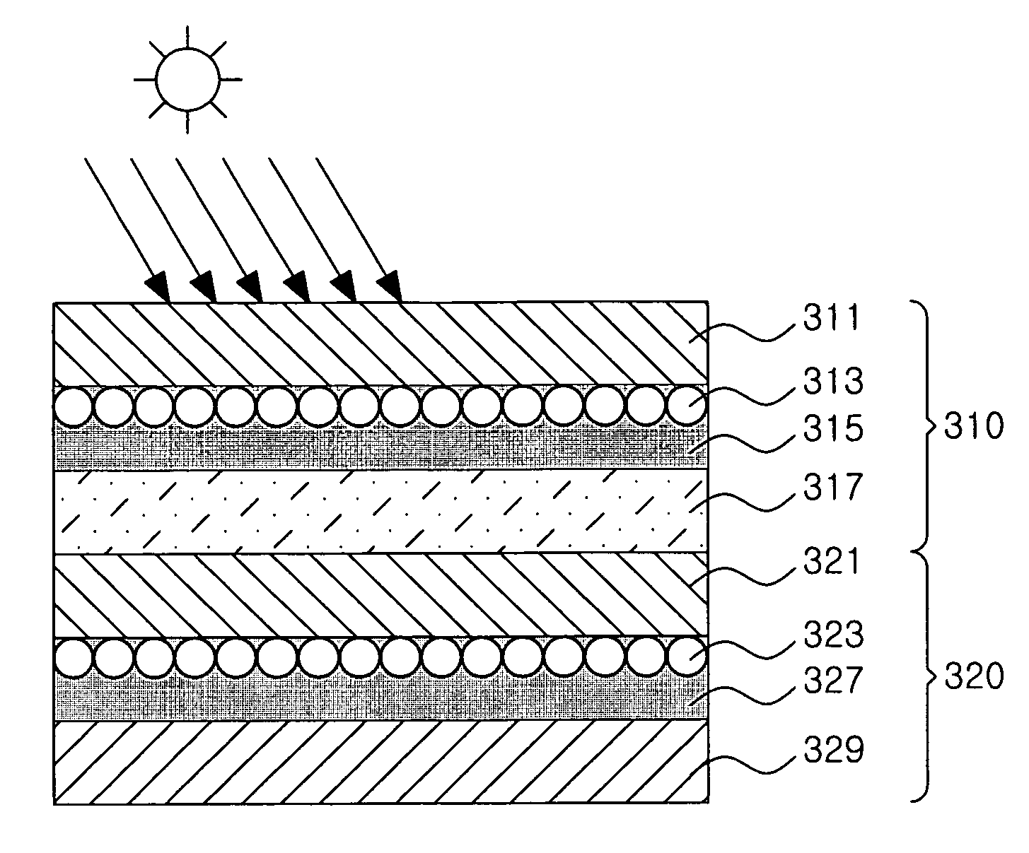
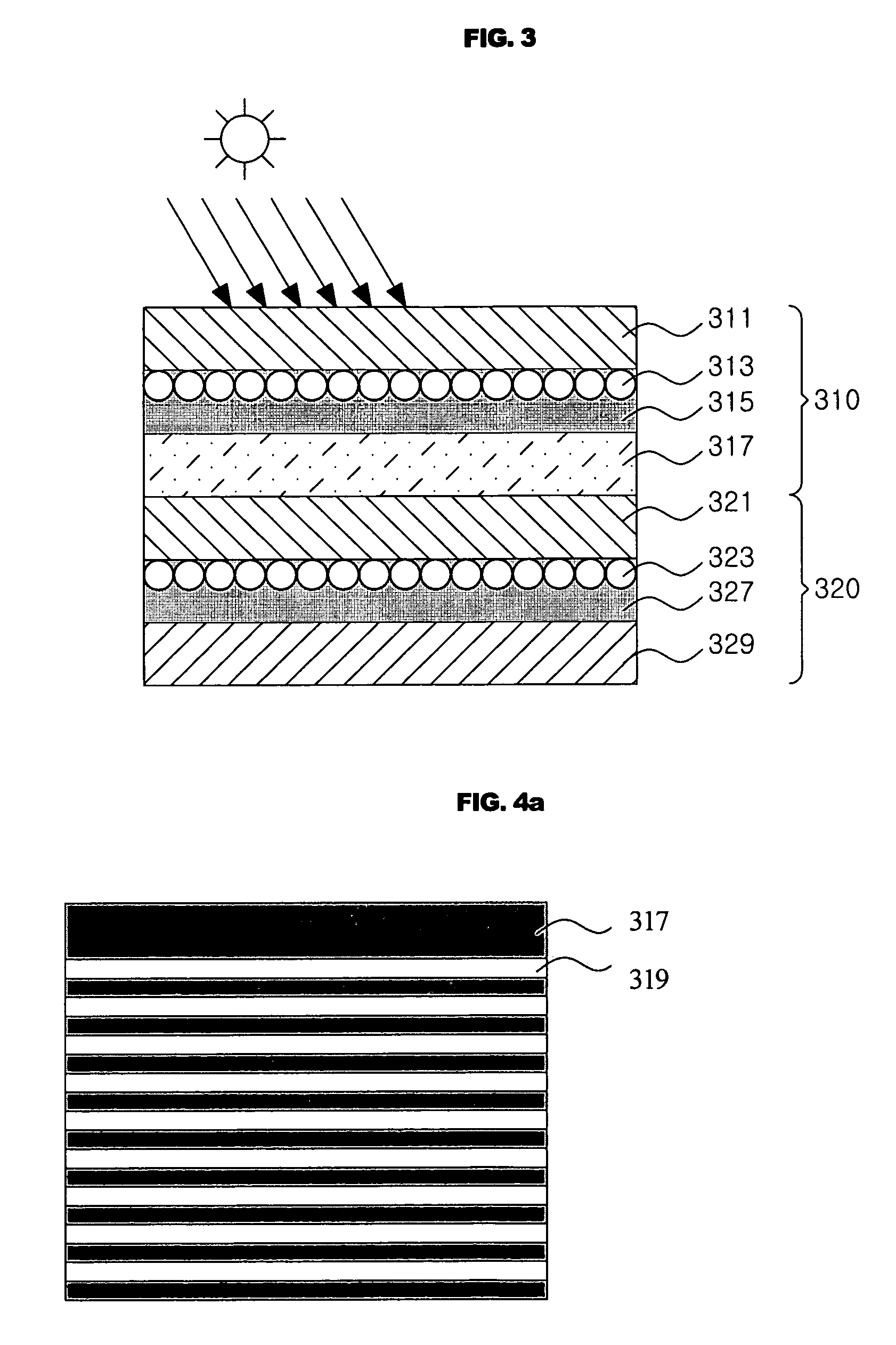
[0085] After fluorine-doped tin oxide (FTO) was applied to a glass substrate using a sputter, a paste of TiO2 particles (average particle diameter: 9 nm) was applied thereto by screen printing and dried at 70° C. for 30 minutes. After drying, the resulting structure was placed in an electric furnace, heated at a rate of 3° C. / min. in air, maintained at 450° C. for 30 minutes, and cooled at a rate of 3° C. / min. to produce a porous TiO2 film having a thickness of about 10 μm. Subsequently, the glass substrate on which the metal oxide layer was formed was dipped in a 0.3 mM ruthenium dithiocyanate 2,2′-bipyridyl-4,4′-dicarboxylate solution for 24 hours and dried to adsorb the dye on the surface of the TiO2 layer. After completion of the adsorption of the dye, ethanol was sprayed to remove the unadsorbed dye and dried, completing formation of a first light-absorbing layer of a first photovoltaic layer. Next, platinum was patterned in a grid shape on an indium tin oxide (ITO)-coated glas...

example 3

[0089] A tandem photovoltaic device was fabricated in the same manner as in Example 2, except that a light-scattering layer was formed on the second transparent electrode of the second photovoltaic layer. At this time, the light-scattering layer was formed by spin coating a metal oxide (TiO2) slurry on the second transparent electrode, followed by annealing.


PUM


Abstract

A tandem photovoltaic device and a method for fabricating the photovoltaic device is disclosed. The tandem photovoltaic device comprises two or more photovoltaic layers laminated to each other, each of which including a semiconductor electrode, an electrolyte layer and a counter electrode. A counter electrode of the upper photovoltaic layer is patterned in a grid shape so as to include a plurality of light-transmitting portions, which permit transmission of light to the lower photovoltaic layer. The tandem photovoltaic device has the advantages of high power conversion efficiency and degree of integration. Advantageously, the tandem photovoltaic device can reduce electric power generation costs.

Description

[0001] This application claims priority to Korean Patent Application No. 2005-91284, filed on Sep. 29, 2005, and all the benefits accruing therefrom under 35 U.S.C. § 119(a), and the contents of which in its entirety are herein incorporated by reference. BACKGROUND OF THE INVENTION [0002] 1. Field of the Invention [0003] The present invention relates to a tandem photovoltaic device and a method for fabricating the photovoltaic device. More particularly, the present invention relates to a tandem photovoltaic device with a high degree of integration and improved power conversion efficiency in which a first counter electrode is patterned to include a plurality of light-transmitting portions, and a method for fabricating the photovoltaic device. [0004] 2. Description of the Related Art [0005] Since solar cells are photovoltaic devices for converting solar energy into electric energy. Solar cells are gradually gaining importance since they utilize inexhaustible solar energy, unlike other...

Claims


Application Information

Patent Timeline
Patent Type & Authority Applications(United States)
IPC IPC(8): H01L31/00
CPCH01G9/2022Y02E10/542H01G9/2072H01G9/2031H01L31/18H01L31/047
Inventor NAM, JUNG GYUPARK, SANG CHEOLPARK, YOUNG JUN
Owner SAMSUNG ELECTRONICS CO LTD
Learn More