Semiconductor memory device

a memory device and semiconductor technology, applied in the field of semiconductor design technologies, can solve the problems of differences in sensing speed and sensing efficiency, and difficulty in amplifying a plurality of cell data for a short tim

Inactive Publication Date: 2007-04-05
SK HYNIX INC
View PDF1 Cites 10 Cited by
  • Summary
  • Abstract
  • Description
  • Claims
  • Application Information

AI Technical Summary

Benefits of technology

[0016] It is, therefore, an object of the present invention to provide a semiconductor memory device which receives a driving voltage of unit bit line sense amplifier supplied from any part therein but is capable of resolving an operational efficiency difference that occurs from a loading difference on a supply line.
[0017] Another object of the present invention is to provide a semiconductor memory device allowing a plurality of unit bit line sense amplifiers to have the same over driving operation efficiency and normal driving operation efficiency.
[0018] Still another object of the present invention is to provide a semiconductor memory device capable of solving a voltage drop problem by pull-up power lines (over driver and normal driver) that are weak in a mesh shape.

Problems solved by technology

As the core voltage that is used for the DRAM operating voltage becomes low, there may be difficulty in amplifying a plurality of cell data for a short time.
Thus, there may be differences between sensing speeds and sensing efficiencies.

Method used


Image

  • Semiconductor memory device
  • Semiconductor memory device
  • Semiconductor memory device

Examples


Embodiment Construction

[0028] Hereinafter, preferred embodiments of the present invention will be set forth in detail with reference to the accompanying drawings to the extent that the invention can be readily carried out by those in the art to which the invention pertains.

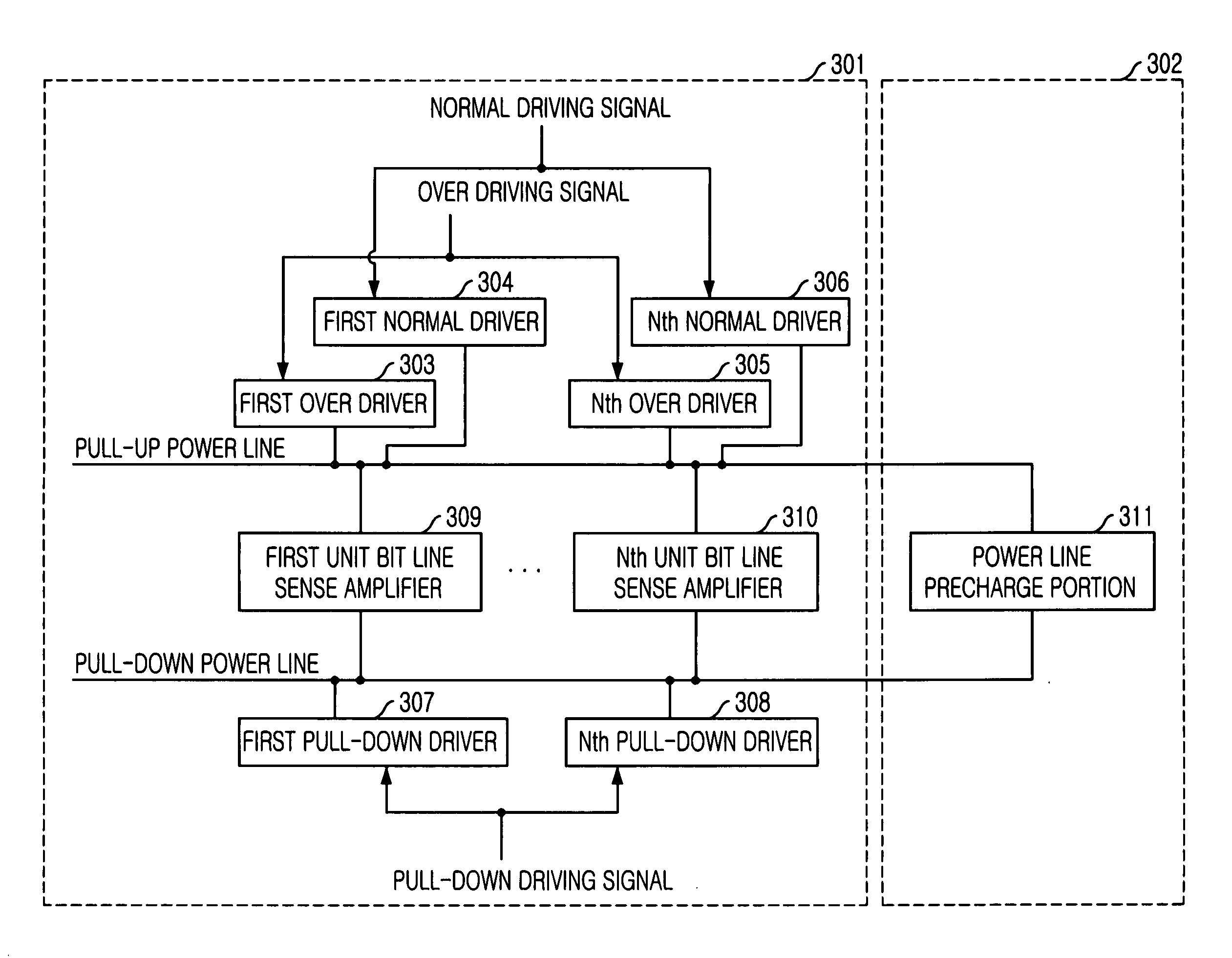
[0029]FIG. 3 is a diagram of a bit line sense amplifier array in accordance with a preferred embodiment of the present invention.

[0030] Referring to FIG. 3, the bit line sense amplifier array 301 includes a plurality of unit bit line sense amplifiers 309 and 310, a plurality of over drivers 303 and 305, a plurality of normal drivers 304 and 306, and a plurality of pull-down drivers 307 and 308 that are configured to correspond to the over drivers 303 and 305 and the normal drivers 304 and 306. In fact, there are provided a plurality (or N-number) of unit bit sense amplifiers, but only the two bit line sense amplifiers prepared at both ends are illustrated for convenience of explanation. The location and number of each of the over driv...


PUM


Abstract

A semiconductor memory device is capable of resolving a problem of operational efficiency difference that can occur due to a loading difference on a supplying line while receiving a driving voltage of a unit bit line sense amplifier supplied from a certain part. The memory device includes a plurality of unit bit line sense amplifiers in a BLSA region, a pull-up power line and a pull-down power line used as power lines of the plurality of unit bit line sense amplifiers, a plurality of normal drivers connected to the pull-up power line at regular intervals in the BLSA region, and a plurality of over drivers connected to the pull-up power line at regular intervals in the BLSA region.

Description

FIELD OF THE INVENTION [0001] The present invention relates to semiconductor design technologies, and more particularly, to a bit line sense amplifier array for use-in a semiconductor memory device. DESCRIPTION OF RELATED ART [0002] In a semiconductor memory device, there is a current trend to reduce power supply voltage due to continuous scaling down of line width and cell size. Hence, a need has existed for design technology to meet the performance required for low voltage environments. [0003] Most of semiconductor memory devices incorporate in a chip an internal voltage generation circuit that accepts an external voltage (power supply voltage) and generates an internal voltage. The memory devices allow the internal voltage generation circuits themselves to supply voltages required for operating circuits within the chip. Among them, in a memory device using a bit line sense amplifier, such as a Dynamic Random Access Memory (DRAM), a core voltage VCORE is employed to sense cell dat...

Claims


Application Information

Patent Timeline
Patent Type & Authority Applications(United States)
IPC IPC(8): G11C7/02
CPCG11C5/063G11C7/1012G11C7/1051G11C7/106G11C7/1075G11C7/1078G11C7/1087G11C7/109
Inventor IM, JAE-HYUKDO, CHANG-HO
Owner SK HYNIX INC
Why Eureka
Try Eureka