Semiconductor memory device

a memory device and semiconductor technology, applied in information storage, static storage, digital storage, etc., can solve the problems of sensor speed and sensing efficiency errors, and the difficulty of amplifying much cell data for a shorter tim

Active Publication Date: 2007-03-29
SK HYNIX INC
View PDF5 Cites 3 Cited by
  • Summary
  • Abstract
  • Description
  • Claims
  • Application Information

AI Technical Summary

Benefits of technology

[0017] It is, therefore, an object of the present invention to provide a semiconductor memory device capable of solving a problem of an operating efficiency difference caused by loading difference of supply line conveying a driving voltage of bit line sense amplifiers.
[0019] Still another object of the present invention is to offer a semiconductor memory device capable of solving a voltage drop problem due to a pull-up power line weak in a mesh shape.

Problems solved by technology

But, in case where only the core voltage is utilized in the DRAM that is under the trend that an operating voltage becomes lower, there may be difficulty in amplifying much cell data for a shorter time.
Thus, there may be errors of sensing speed and sensing efficiency.

Method used


Image

  • Semiconductor memory device
  • Semiconductor memory device
  • Semiconductor memory device

Examples


Embodiment Construction

[0030] Hereinafter, a preferred embodiment of the present invention will be set forth in detail with reference to the accompanying drawings so that the invention can be readily carried out by those in the art to which the invention pertains.

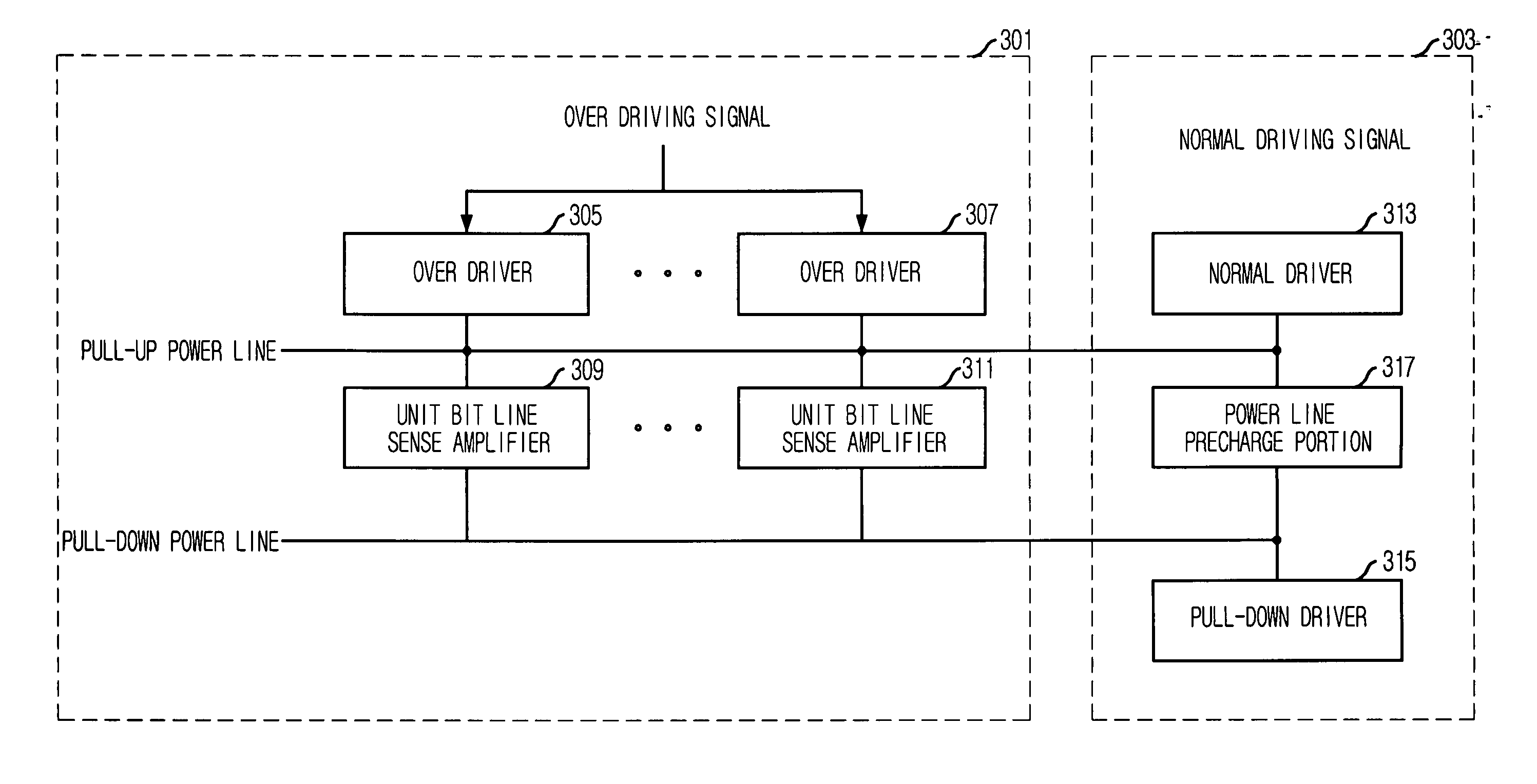
[0031]FIG. 3 is a view illustrating a concept of a bit line sense amplifier array in accordance with an embodiment of the present invention.

[0032] As shown in FIG. 3, the bit line sense amplifier array 301 includes a plurality of unit bit line sense amplifiers 309 and 311, and a plurality of over drivers 305 and 307, which is configured to correspond to the positions and the number of the plurality of unit bit line sense amplifiers 309 and 311. The number of the unit bit line sense amplifiers is determined within a range that its operation efficiency is not decreased by loading difference of the power lines of the bit line sense amplifiers connected in parallel.

[0033] In addition, within a sub-hall area 303 for controlling the bit line sense a...


PUM


Abstract

Provided are semiconductor design technologies, especially a bit line sense amplifier array of a semiconductor memory device. The semiconductor memory device includes a plurality of unit bit line sense amplifiers, a pull-up power line which is a power line of the plurality of unit bit line sense amplifiers, a single normal driver prepared on one side of the pull-up power line, and a plurality of over drivers arranged at regular intervals and partially connected to the pull-up power line.

Description

FIELD OF THE INVENTION [0001] The present invention relates to semiconductor design technologies; and, more particularly, to a bit line sense amplifier array of a semiconductor memory device. DESCRIPTION OF RELATED ART [0002] In a semiconductor memory device, it is a current trend that a voltage reduction of a power supply voltage is accelerating due to progressing of continuous scaling down of line width and cell size. According to this, a need has existed for design technology to meet the performance required in the low voltage environment. [0003] Most semiconductor memory devices incorporate in a chip an internal voltage generating circuit that accepts an external voltage (power supply voltage) and generates an internal voltage. As a result, those devices themselves allow supply of voltages required for operating of circuits inside the chip. Among them, in a memory device using a bit line sense amplifier such as Dynamic Random Access Memory (DRAM), a core voltage VCORE is used to...

Claims


Application Information

Patent Timeline
Patent Type & Authority Applications(United States)
IPC IPC(8): G11C5/06
CPCG11C5/025G11C5/063G11C2207/065G11C11/4074G11C11/4091G11C7/065
Inventor IM, JAE-HYUKDO, CHANG-HO
Owner SK HYNIX INC
Why Eureka
Try Eureka