Structure of integrated circuit standard cell library for reducing power supply voltage fluctuation

a technology of integrated circuits and library circuits, applied in the direction of program control, instrumentation, and semiconductor/solid-state device details, can solve problems such as unsatisfactory voltage fluctuations, and achieve the effect of resisting voltage drop problems

Inactive Publication Date: 2005-06-28
TAIWAN SEMICON MFG CO LTD
View PDF7 Cites 4 Cited by
  • Summary
  • Abstract
  • Description
  • Claims
  • Application Information

AI Technical Summary

Benefits of technology

[0018]In this manner the current supplied by the power supply connected to the first and second power buses is shared between the first power bus and the second power bus and resistance voltage drop problems on the first power bus and second power bus are minimized.

Problems solved by technology

Current fluctuations in the cells due to switching voltages applied to the signal input 119 of the cells will cause undesirable voltage fluctuations to occur on the VDD supply bus, due to resistance voltage drops on the VDD supply bus, which will cause undesirable voltage fluctuations at the output terminal 150 of the row of cells.

Method used


Image

  • Structure of integrated circuit standard cell library for reducing power supply voltage fluctuation
  • Structure of integrated circuit standard cell library for reducing power supply voltage fluctuation
  • Structure of integrated circuit standard cell library for reducing power supply voltage fluctuation

Examples


Embodiment Construction

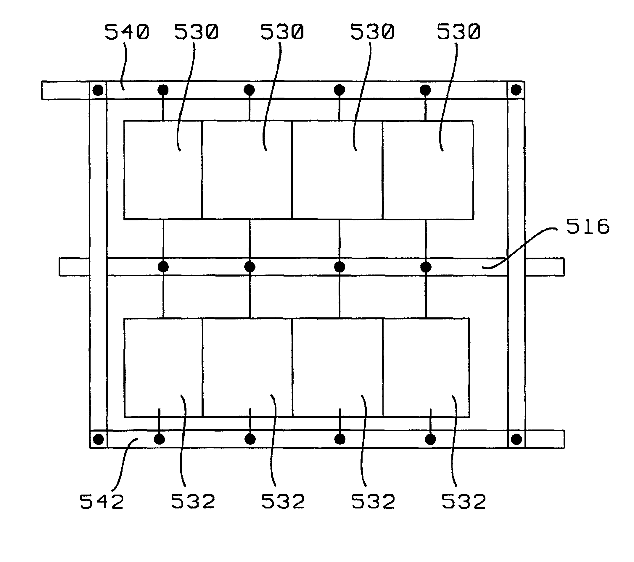
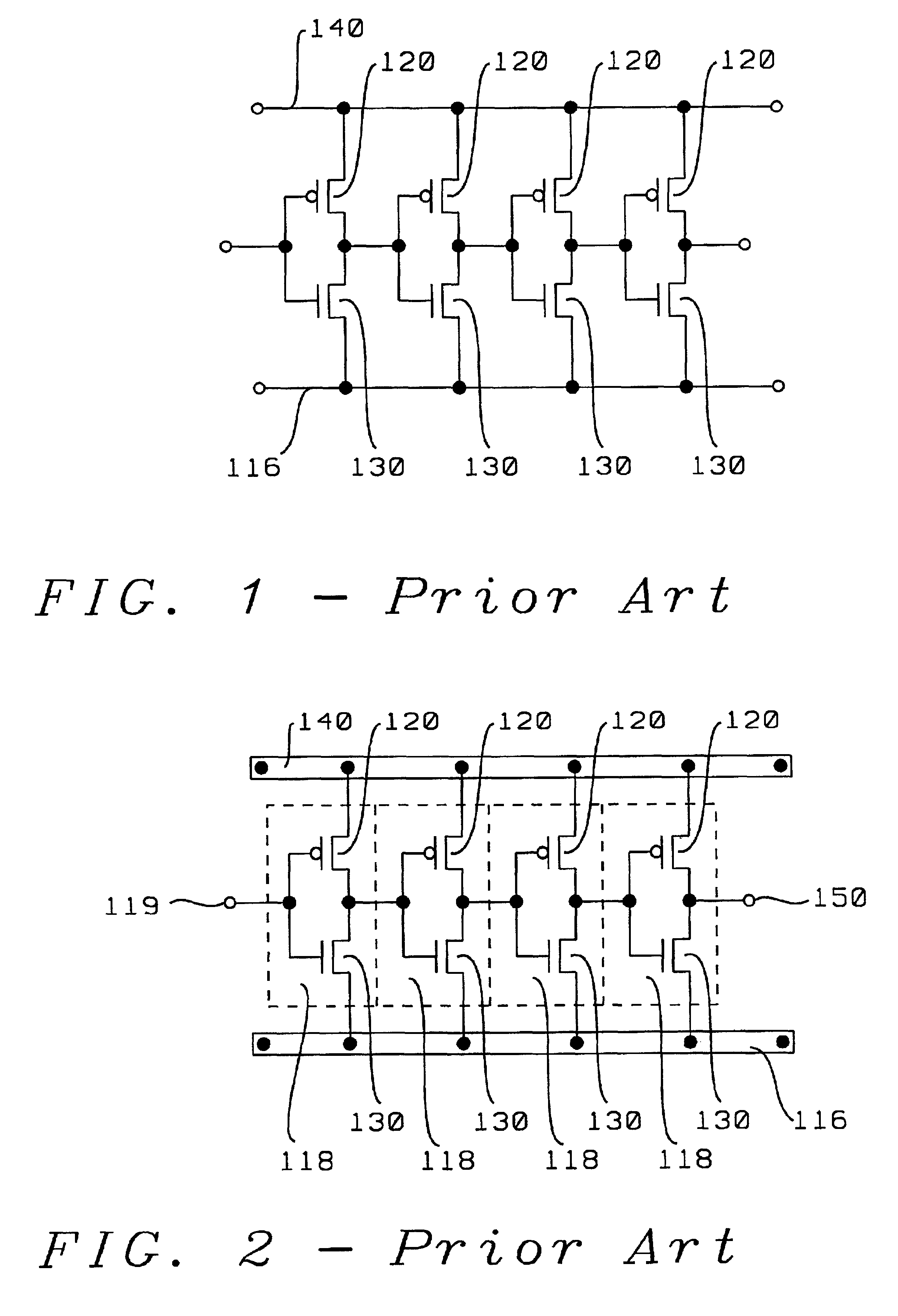
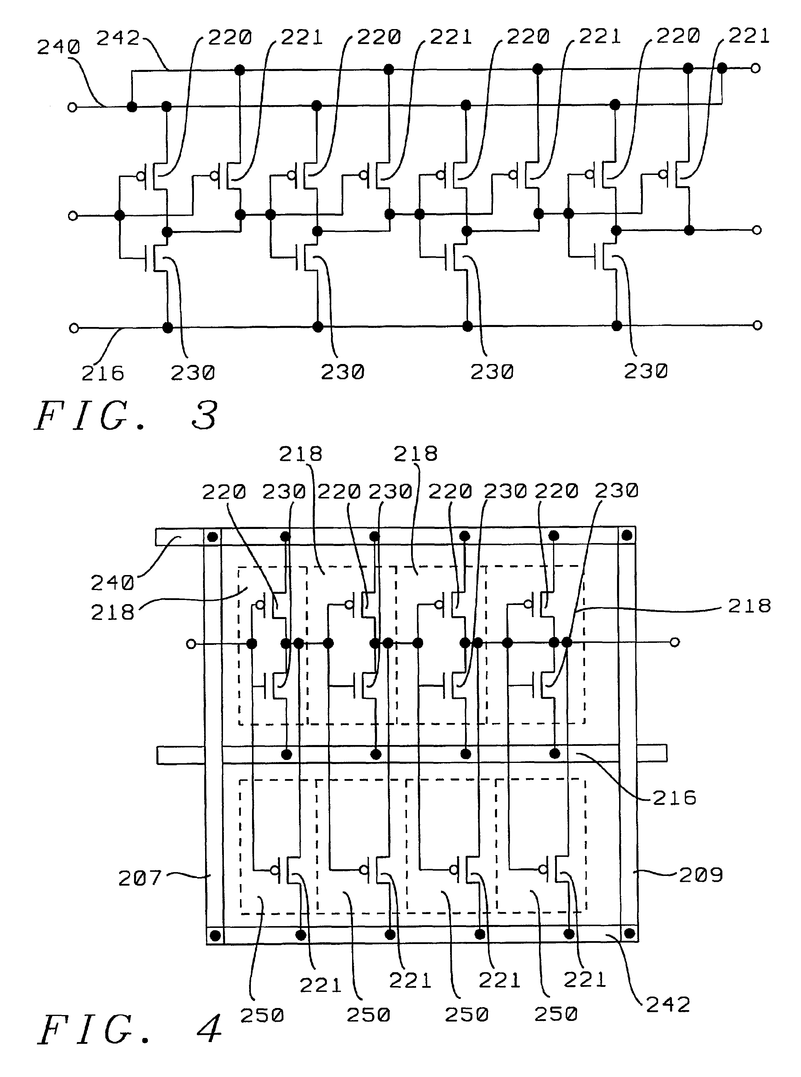
[0026]Refer now to FIGS. 3-5 for the layout structure this invention. FIG. 3 shows a schematic diagram of the circuit resulting from partitioning the circuit of FIG. 1 according to the layout structure and method of this invention. Each of the P channel FETs 120 shown in FIG. 1 are replaced by a parallel combination of a first P channel FET 220 and a second P channel FET 221, as shown in FIG. 3. Each of the N channel FETs 130 shown in FIG. 1 are remain as a single N channel FET 230 as shown in FIG. 3. The single VDD power supply bus 140 shown in FIG. 1 is replaced by a first power bus 240 and a second power bus 242 as shown in FIG. 3. As shown in FIG. 3 the sources of the first P channel FETs 220 are connected to the first power bus 240 and the sources of the second P channel FETs 221 are connected to the second power bus 242. Also as shown in FIG. 3, the sources of the N channel FETs 230 are connected to a second power bus 216. The first power bus 240 and second power bus 242 are e...


PUM


Abstract

A layout structure and method are described for the layout of chips having libraries of standard cells which minimizes voltage fluctuations on power buses caused by switching circuits in the standard cells. Typically these standard cells are arranged in a row between two power buses. In this invention the standard cells are partitioned into first cells and second cells which can be combined to form the standard cell circuit. The first cells are arranged in a first row and the second cells are arranged in a second row. A first power bus is located above the first row of first cells and a second power bus is located below the second row of second cells. The first power bus and second power bus are electrically connected together. The first power bus supplies a first power supply voltage to the first cells and the second power bus supplies the first power supply voltage to the second cells. A third power bus is located between the first row of first cells and second row of second cells and supplies a second power supply voltage to the first and second cells. The layout can be accomplished automatically using a computer program.

Description

BACKGROUND OF THE INVENTION[0001](1) Field of the Invention[0002]This invention relates to a layout structure for standard cell or library circuit cells which reduce fluctuations in power supply voltage supplied to the cells due to large current swings.[0003](2) Description of the Related Art[0004]Power and ground voltages are typically supplied to integrated circuit devices by power buses. Frequently the current fluctuations in these buses, caused by circuit switching, cause fluctuations in the voltage actually delivered to the devices. A number of workers have described methods to minimize the fluctuations in the power supply voltage actually delivered to these devices due to current fluctuations in the power supply buses.[0005]U.S. Pat. No. 4,811,237 to Putatunda et al. describe an integrated circuit chip layout arrangement using an interlocking power bus mesh structure.[0006]U.S. Pat. No. 5,391,900 to Onodera et al. describe an integrated circuit chip design having at least one ...

Claims


Application Information

Patent Timeline
Patent Type & Authority Patents(United States)
IPC IPC(8): G06F9/45G06F17/50H01L27/118
CPCH01L27/11803G06F17/5068G06F30/39
Inventor WANG, SHAO-YUWU, CHIEN-TEHSIAO, JUN-JYEH
Owner TAIWAN SEMICON MFG CO LTD
Why Eureka
Try Eureka