
Plasma display panel

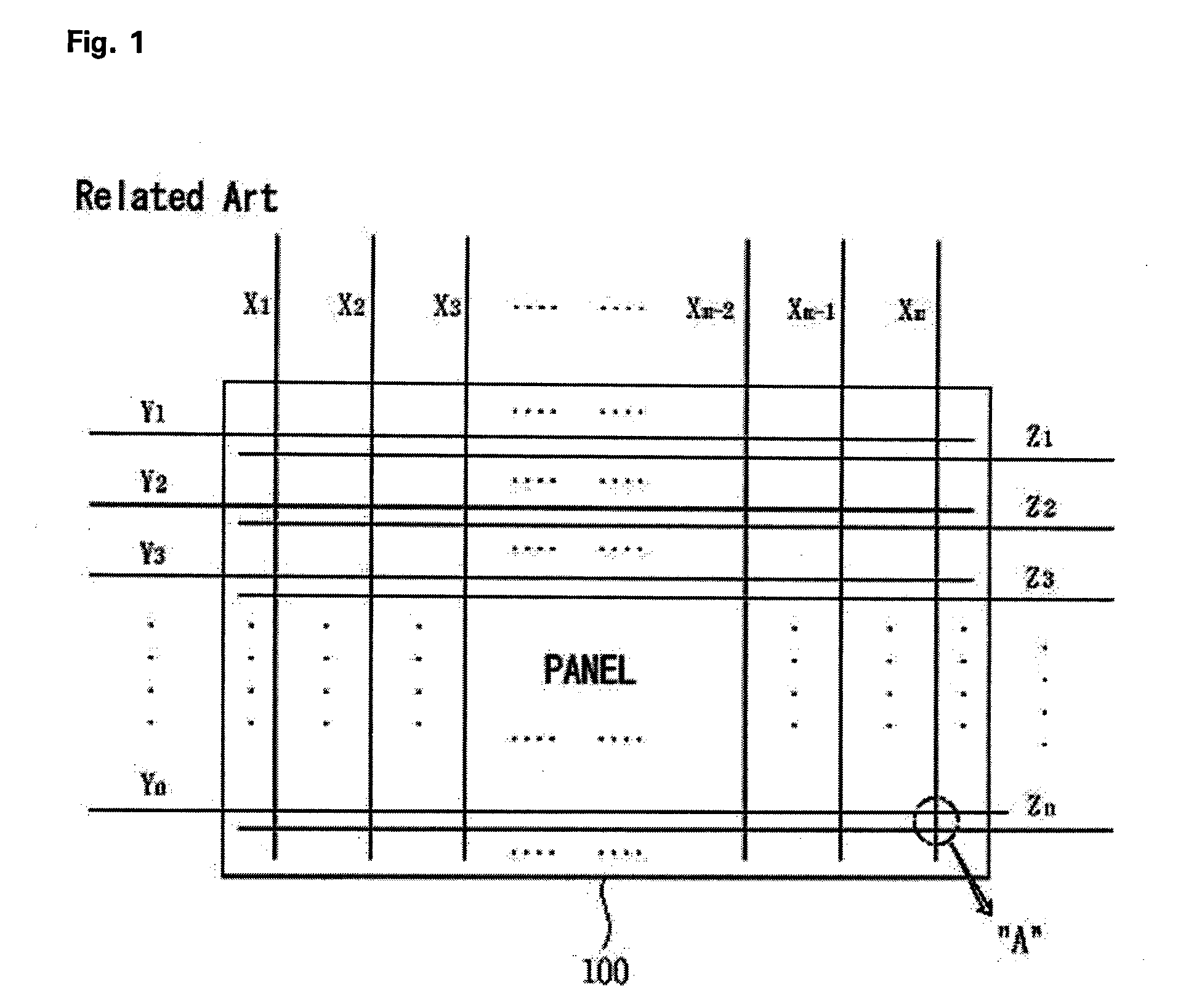
a technology of display panel and plasma, which is applied in the direction of gas discharge vessel/container, electrode, gas-filled discharge tube, etc., can solve the problems of deteriorating jitter characteristic, prolonged discharge time, and erroneous discharge, so as to enhance the driving efficiency of the panel, improve the jitter characteristic, and increase the accuracy of the discharge

Inactive Publication Date: 2007-04-12
LG ELECTRONICS INC
View PDF30 Cites 1 Cited by
  • Summary
  • Abstract
  • Description
  • Claims
  • Application Information

AI Technical Summary

Benefits of technology

[0013] It is an object of the present invention to provide a plasma display panel in which an erroneous discharge is prevented and the accuracy of a discharge increases.
[0022] The plasma display panel according to an embodiment of the present invention is advantageous in that it improves luminance.

Problems solved by technology

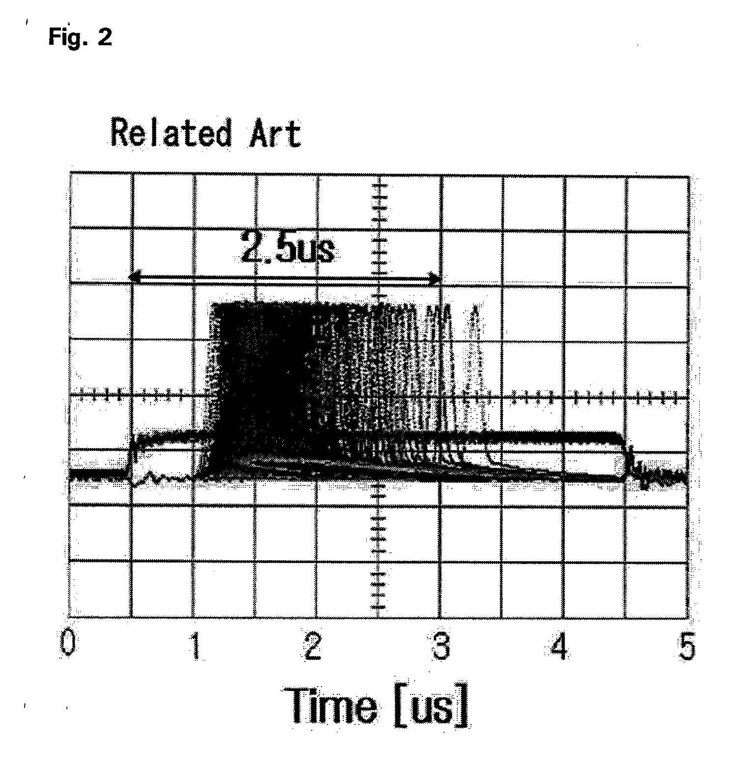
Therefore, a problem arises in that a discharge times become prolonged, i.e., a problem whereby a jitter characteristic deteriorates.
A delayed discharge due to a worsened jitter characteristic adversely effects the next discharge, thereby resulting in an erroneous discharge.
For example, a jitter characteristic may deteriorate due to a difference in an amount of wall charges between electrodes, a weak discharge between electrodes is generated, inaccuracy of a discharge between target electrodes and / or the like.

Method used


Image

  • Plasma display panel
  • Plasma display panel
  • Plasma display panel

Examples


first embodiment

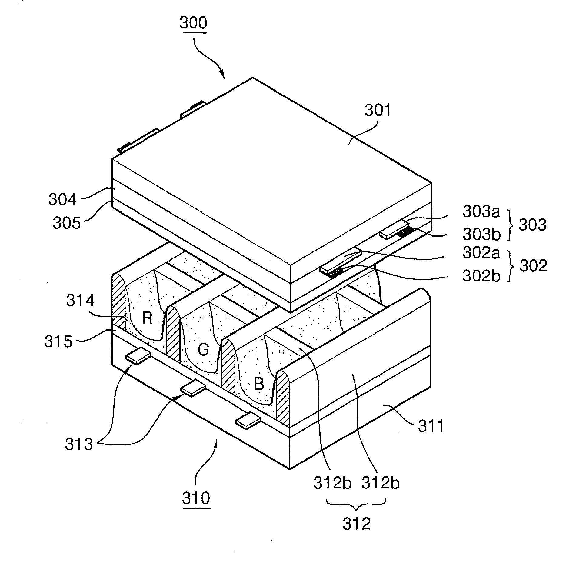
[0087] The plasma display panel according to the present invention further comprises an address electrode 313 intersecting the scan electrode 302 or the sustain electrode 303. A discharge cell is formed at a region where the scan electrode 302 or the sustain electrode 303 intersects the address electrode 313.

[0088] The electrode structure corresponding to one discharge cell has been shown in FIG. 6 in detail. A first width (W1) in the longitudinal direction of the address electrode 313 of the scan transparent electrode 302a is wider than a second width (W2) in the longitudinal direction of the address electrode 313 of the sustain transparent electrode 303a, in a region within the discharge cell.

[0089] The first width (W1) is 5% to 50% wider than the second width (W2). More particularly, the width (W1) in the longitudinal direction of the address electrode 313 of the scan transparent electrode 302a is 10% to 30% wider than the width (W2) in the longitudinal direction of the address ...

second embodiment

[0102] The scan transparent electrode 302a and the sustain bus electrode 303a are shown in FIG. 9. However, the present invention can be implemented using only the scan bus electrode 302b and the sustain bus electrode 303b without the scan transparent electrode 302a and the sustain bus electrode 303a.

[0103] The plasma display panel according to a second embodiment of the present invention further comprises an address electrode 313 intersecting the scan electrode 302 or the sustain electrode 303. A discharge cell is formed at a location where the scan electrode 302 or the sustain electrode 303 intersects the address electrode 313.

[0104] In FIG. 9, a first width (W5) in the longitudinal direction of the address electrode 313 of the scan bus electrode 302b is set to be wider than a second width (W6) in the longitudinal direction of the address electrode 313 of the sustain bus electrode 303b, in a region within the discharge cell.

[0105] That is, for example, the first width (W5) is f...

third embodiment

[0111]FIG. 10 shows an electrode structure of a plasma display panel according to the present invention. As shown in FIG. 10, a width (W1) in the longitudinal direction of an address electrode 313 of a scan transparent electrode 302a is formed wider than a width (W2) in the longitudinal direction of the address electrode 313 of a sustain transparent electrode 303a. A width (W5) in the longitudinal direction of the address electrode 313 of a scan bus electrode 302b is formed wider than a width (W6) in the longitudinal direction of the address electrode 313 of a sustain bus electrode 303b. The scan transparent electrode 302a and the sustain transparent electrode 303a and the scan bus electrode 302b and the sustain bus electrode 303b have been described in detail above. Therefore, description thereof will be omitted to avoid redundancy.

[0112] As described above, the plasma display panel of the present invention can improve a jitter characteristic by controlling the width of electrodes....


PUM


Abstract

The present invention relates to a plasma display panel including electrodes. In the plasma display panel according to an embodiment of the present invention, an area of a scan electrode is larger than that of a sustain electrode. Therefore, a jitter characteristic improves.

Description

CROSS-REFERENCES TO RELATED APPLICATIONS [0001] This Nonprovisional application claims priority under 35 U.S.C. § 119(a) on Patent Application No. 10-2005-0085461 filed in Korea on Sep. 13, 2005 the entire contents of which are hereby incorporated by reference. BACKGROUND OF THE INVENTION [0002] 1. Field of the Invention [0003] The present document relates to a plasma display panel. [0004] 2. Background of the Related Art [0005] A general plasma display panel comprises a plurality of barrier ribs that are formed between a front panel and a rear panel and partition discharge cells. A plurality of discharge cells forms one pixel. For example, a red (R) cell, a green (G) cell and a blue (B) cell form one pixel. [0006] Each discharge cell is filled with an inert gas containing a primary discharge gas, such as neon (Ne), helium (He) or a mixed gas of Ne+He, and a small amount of xenon (Xe). If a high frequency voltage discharges the inert gas, vacuum ultraviolet rays are radiated. Vacuum...

Claims


Application Information

Patent Timeline
Patent Type & Authority Applications(United States)
IPC IPC(8): H01J17/49H01J11/12H01J11/22H01J11/24H01J11/26H01J11/34H01J11/36H01J11/38H01J11/40H01J11/42H01J11/50
CPCH01J2211/365H01J2211/54H01J11/12H01J11/24H01J2211/245H01J11/26H01J11/36
Inventor PARK, CHUNG HOORYU, SEONG NAMCHOI, JOON YOUNG
Owner LG ELECTRONICS INC
Learn More