Repair circuit of semiconductor memory device

Active Publication Date: 2007-04-12
SK HYNIX INC
View PDF3 Cites 1 Cited by
  • Summary
  • Abstract
  • Description
  • Claims
  • Application Information

AI Technical Summary

Benefits of technology

[0018] An embodiment of the present invention is that it provides a repair circuit of a semiconductor memory device, in which if an address on which a repair operation must be performed occurs, the operating speed of the repair cell is made faster than that of a normal cell, thereby improving the operating speed of the device.

Problems solved by technology

To discard the whole device as a failed product despite the fact that only several cells within the memory have failed, however, is inefficient in terms of the yield.
There is a limit to a reduction of a time which is taken for the repair controller to operate.
If the spec defining the data I / O time is reduced, the desirable spec of the device cannot be obtained due to the operating time of the repair controller.
Therefore, they do not satisfy the spec of the device for the I / O time.

Method used


Image

  • Repair circuit of semiconductor memory device
  • Repair circuit of semiconductor memory device
  • Repair circuit of semiconductor memory device

Examples


Embodiment Construction

[0030] The present invention will now be described in detail in connection with certain exemplary embodiments with reference to the accompanying drawings.

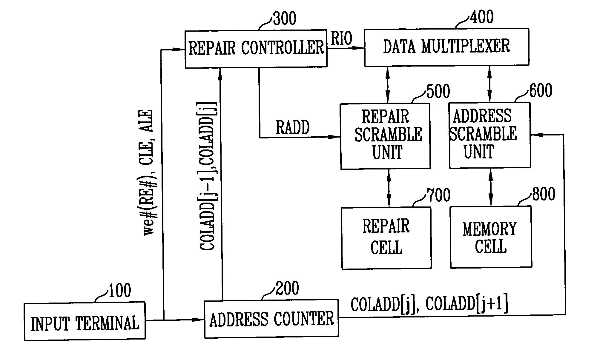
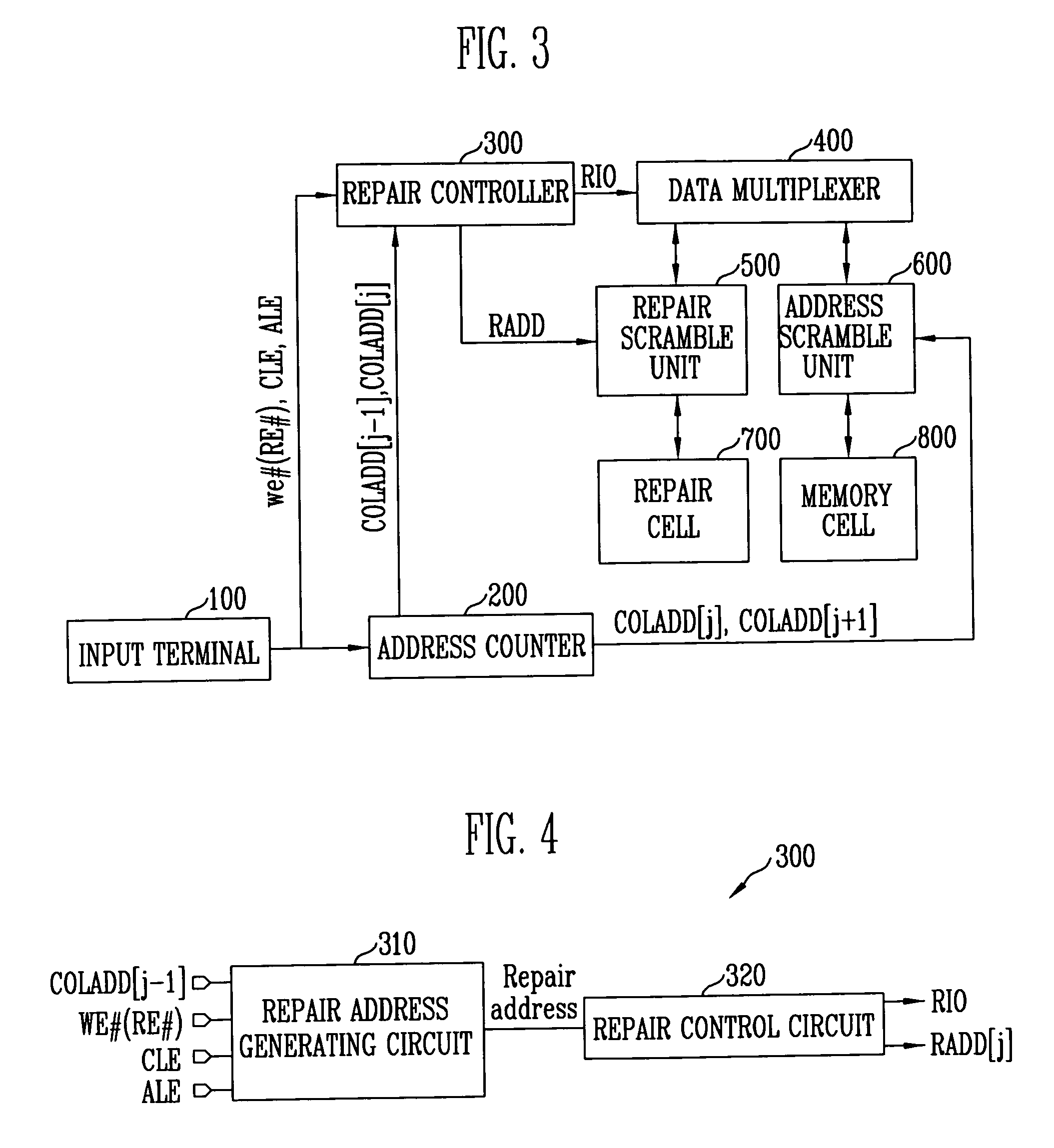
[0031]FIG. 3 is a block diagram of a repair circuit of a semiconductor memory device according to an embodiment of the present invention.

[0032] Referring to FIG. 3, input signals (i.e., a write enable signal WE# or a read enable signal RE#, an address latch enable signal ALE, and a command latch enable signal CLE) are input through an input terminal 100, and are then transmitted to an address counter 200 and a repair controller 300.

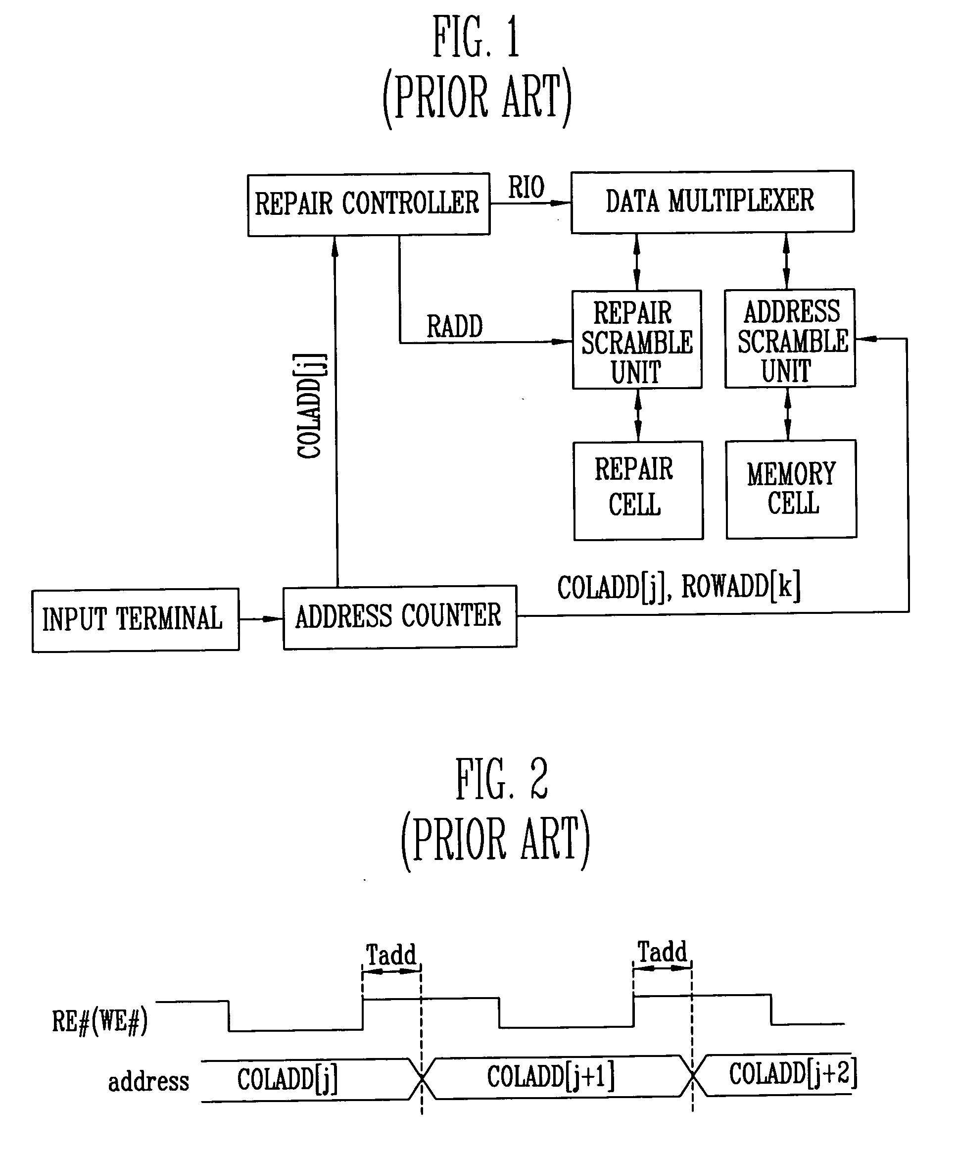
[0033] The address counter 200 outputs column address signals COLADD[j], COLADD[j+1] whose addresses have been increased whenever the write enable signal WE# or the read enable signal RE# is toggled.

[0034] The repair controller 300 outputs a repair control signal RIO and a repair address signal RADD in response to the write enable signal WE# or the read enable signal RE#, the address latch enable sig...


PUM


Abstract

An embodiment of the present invention relates to a repair circuit of a semiconductor memory device. The repair circuit includes an address counter that sequentially generates a first column address signal and a second column address signal in response to a write enable signal or a read enable signal, a repair controller that generates a repair column address signal earlier than the second column address signal in response to the first column address signal, an address latch enable signal, a command enable signal, and a write enable signal, and a repair scramble unit that selects a repair cell in response to a repair I / O control signal and the repair column address signal. If an address on which a repair operation must be performed occurs, the repair controller directly receives the write enable signal or the read enable signal and activates the repair controller earlier than a general cell using a previous address, thereby offsetting an operating time consumed in the repair controller. Therefore, the operating speed of the repair cell can become faster than that of the general cell and the operating speed of the device can be improved accordingly.

Description

BACKGROUND [0001] 1. Field of the Invention [0002] The present invention generally relates to a repair circuit of a semiconductor memory device, and more particularly, to a repair circuit of a semiconductor memory device, in which it can prevent a repair cell from operating slower than a normal memory cell. [0003] 2. Discussion of Related Art [0004] A semiconductor memory device does not function as a memory device if even one of many delicate cells fails. To discard the whole device as a failed product despite the fact that only several cells within the memory have failed, however, is inefficient in terms of the yield. [0005] Currently, the memory device is restored by replacing a failed normal unit cell with a reservation unit cell that is previously provided in the memory device in order to improve the yield. [0006]FIG. 1 is a block diagram illustrating the process of performing the repair operation in the related art. FIG. 2 is a timing diagram of signals illustrating the addres...

Claims


Application Information

Patent Timeline
IPC IPC(8): G11C29/00
CPCG11C29/842G11C29/846G11C29/00
Inventor PARK, YOUNG SOO
Owner SK HYNIX INC
Why Eureka
Try Eureka