Single-mask fabrication process for linear and angular piezoresistive accelerometers

a piezoresistive accelerometer and fabrication process technology, applied in the field of single-mask fabrication of piezoresistive accelerometers, can solve the problems of not knowing the prior art, piezoresistive accelerometers have never before been fabricated using a single mask, etc., and achieve the effect of reducing both complexity and cost and less temperature sensitive sensors

Active Publication Date: 2007-04-19
RGT UNIV OF CALIFORNIA
View PDF4 Cites 17 Cited by
  • Summary
  • Abstract
  • Description
  • Claims
  • Application Information

AI Technical Summary

Benefits of technology

[0010] The illustrated embodiment of the invention is a method for fabricating piezoresistive accelerometers. Normally multiple masks are required when fabricating piezoresistive accelerometers. By utilizing silicon-on-insulator (SOI) wafers with a selected resistivity, ...

Problems solved by technology

No prior art is known to exist where wafers with a selected resistivity are utilized to accomplish piezoresistive accelerometers without...

Method used


Image

  • Single-mask fabrication process for linear and angular piezoresistive accelerometers
  • Single-mask fabrication process for linear and angular piezoresistive accelerometers
  • Single-mask fabrication process for linear and angular piezoresistive accelerometers

Examples


Embodiment Construction

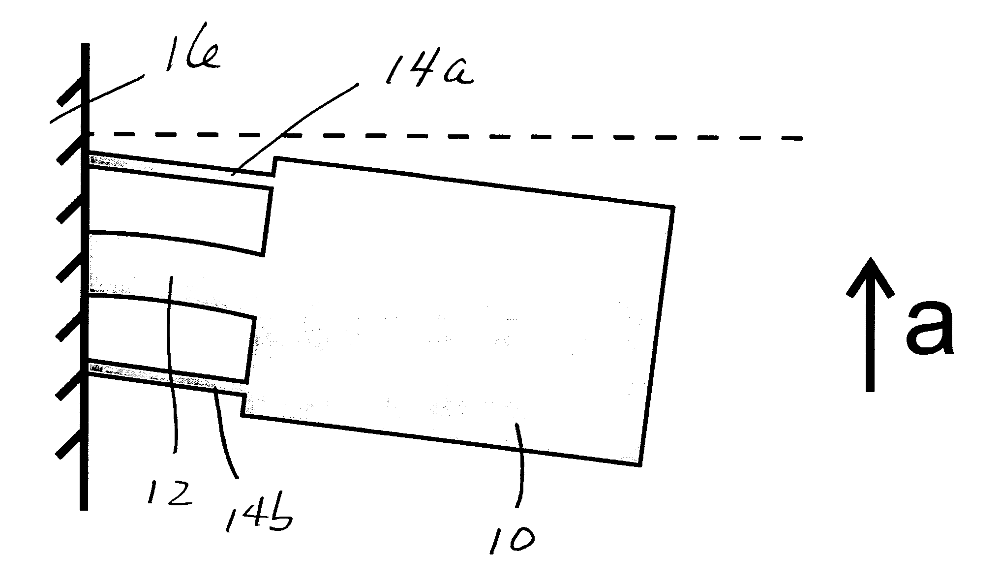
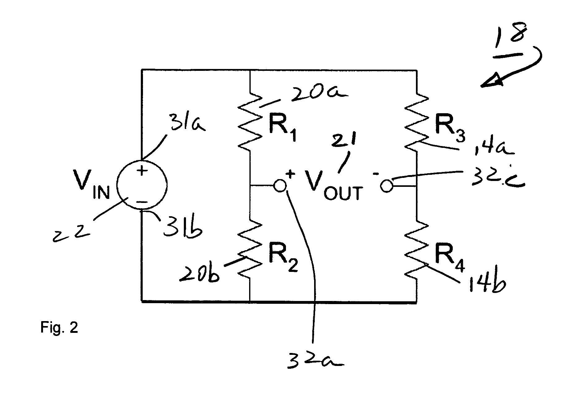
[0031] The illustrated embodiment is a method for fabricating piezoresistive accelerometers based on using Silicon-on-Insulator (SOI) wafers. By choosing wafers with a certain resistivity, the need for doping steps can be eliminated from the fabrication process and the devices can be fabricated using only a single photomask. Below we provide a description of piezoresistivity and the operation of piezoresistive accelerometers and then the illustrated embodiment of the invention is described in detail.

[0032] Piezoresistivity

[0033] Assume that a force is applied to the end of a long isotropic bar. The stress, σ, is then defined as F / A, where F is the applied force, and A the cross-sectional area. The resulting strain, ε, is the change in length divided by the initial length, ΔL / L0. As long as the strain is not too large, many solid materials behave like linear springs, meaning that the displacement is proportional to the applied force or acceleration. The piezoresistive effect causes...


PUM

PropertyMeasurementUnit
Electrical resistanceaaaaaaaaaa
Electrical resistivityaaaaaaaaaa

Abstract

An accelerometer and a method of fabricating an integrated accelerometer comprises the steps of providing an SOI wafer with a selected resistivity to eliminate any need for additional doping of the SOI wafer, providing a single mask on the SOI wafer, and simultaneously defining all components of the accelerometer in the SOI wafer without using any pn-junctions to define any piezoresistive components and to provide the same resistivity of all components. The step of simultaneously defining all components of the accelerometer in the SOI wafer comprises defining all components of a linear or angular accelerometer.

Description

RELATED APPLICATIONS [0001] The present application is related to U.S. Provisional Patent Application, Ser. No. 60 / 726,684, filed on Oct. 13, 2005, and Ser. No. 60 / 726,723, filed on Oct. 13, 2005, which are incorporated herein by reference and to which priority is claimed pursuant to 35 USC 119.BACKGROUND OF THE INVENTION [0002] 1. Field of the Invention [0003] The invention relates to the field of the methods for fabricating piezoresistive accelerometers. [0004] 2. Description of the Prior Art [0005] The fabrication of piezoresistive accelerometers is well known. While silicon-on-insulator (SOI) wafers have previously been utilized to fabricate piezoelectric accelerometers, these prior art processes use comparatively complex fabrication steps that require multiple masks and additional doping of the wafers. Examples of such processes are disclosed in Partridge et.al. “A High-Performance Planar Piezoresistive Accelerometer”, Journal of Microelectromechanical Systems, Vol. 9, No. 1, p...

Claims


Application Information

Patent Timeline
IPC IPC(8): H01S4/00
CPCG01P15/0802G01P15/0888Y10T29/49002G01P2015/0817G01P15/123
Inventor EKLUND, E. JESPERSHKEL, ANDRIE M.
Owner RGT UNIV OF CALIFORNIA
Why Eureka
Try Eureka