Display device and fabricating method thereof

a display device and fabrication method technology, applied in the field of display devices, can solve the problems of large discharge cell size, difficult to implement high resolution in a small-sized display device using the conventional pdp, and complex structure of conventional pdp fabrication, etc., and achieve the effect of simple and efficient structure and high resolution

Inactive Publication Date: 2007-04-26
SAMSUNG SDI CO LTD
View PDF19 Cites 3 Cited by
  • Summary
  • Abstract
  • Description
  • Claims
  • Application Information

AI Technical Summary

Benefits of technology

[0008] Aspects of the present invention provide a display device capable of implementing a high resolution while having a simple and efficient structure and a method of fabricating the same.

Problems solved by technology

However, the conventional PDP is complex in structure because it requires many processes for forming the electrodes and the front and rear substrates are attached and sealed using frit.
Accordingly, the conventional PDP is complex to fabricate and large in the size of the discharge cell.
Therefore, it is difficult to implement high resolution in a small-sized display device using the conventional PDP.

Method used


Image

  • Display device and fabricating method thereof
  • Display device and fabricating method thereof
  • Display device and fabricating method thereof

Examples


Embodiment Construction

[0033] Reference will now be made in detail to the present embodiments of the present invention, examples of which are illustrated in the accompanying drawings, wherein like reference numerals refer to the like elements throughout. The embodiments are described below in order to explain the present invention by referring to the figures.

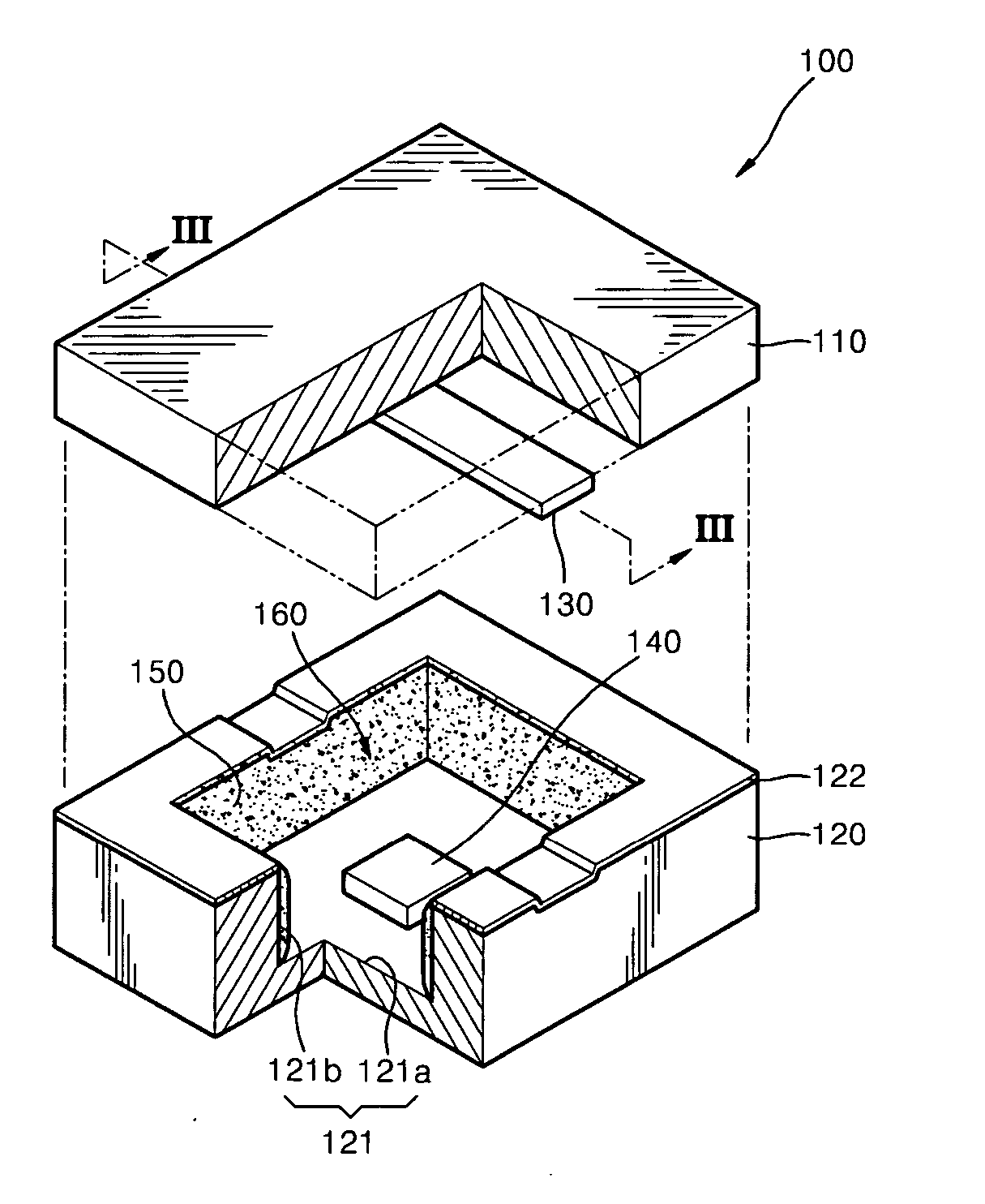
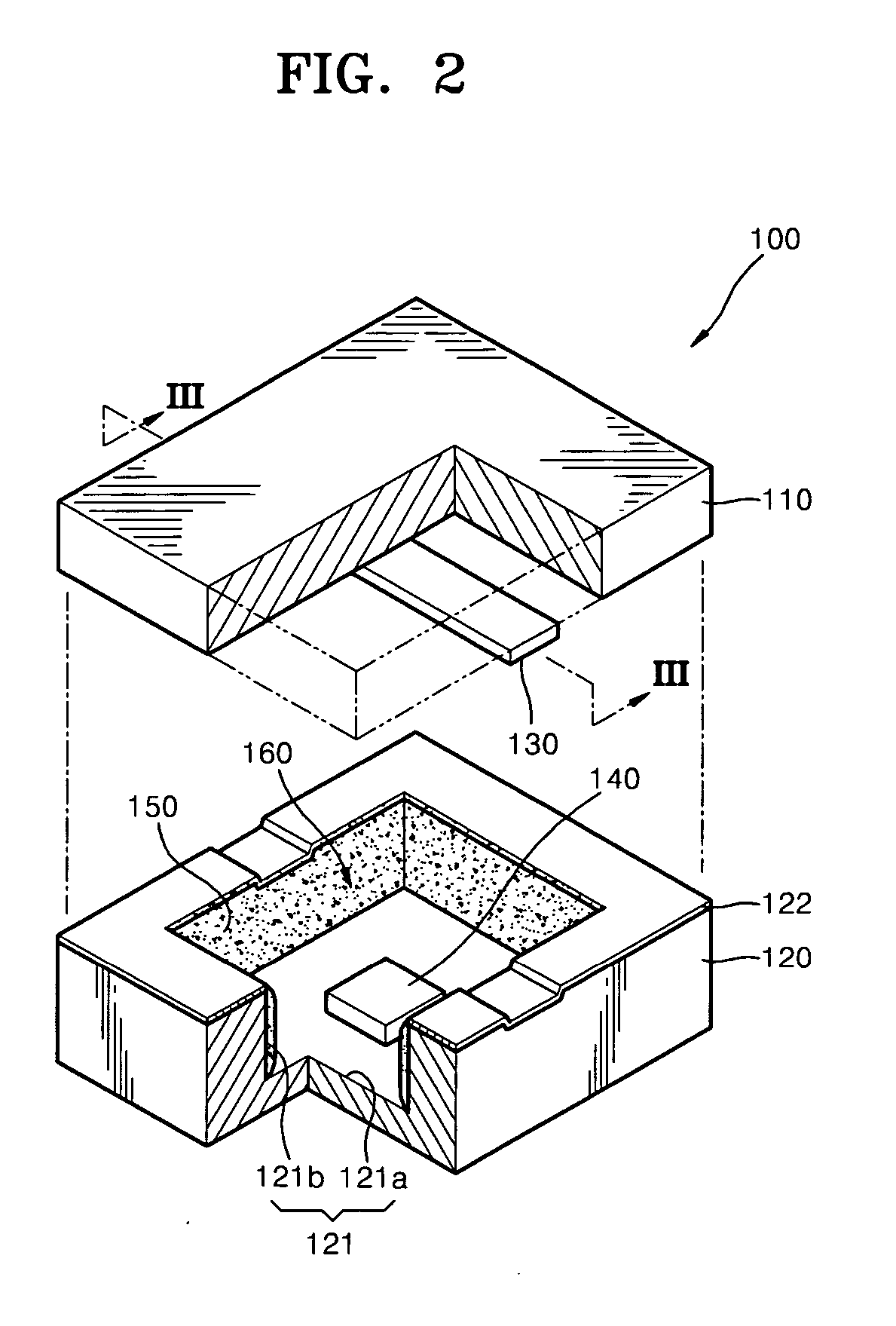
[0034]FIG. 2 is a cutaway perspective view of a display device according to an embodiment of the present invention, FIG. 3 is a sectional view taken along line III-III of FIG. 2, and FIG. 4 is a right side view of the display device illustrated in FIG. 2. Referring to FIGS. 2 through 4, a display device 100 includes a substrate 110, a silicon member 120, an anode electrode 130, an electron emission member 140, and a phosphor layer 150.

[0035] The substrate 110 is formed of transparent glass, and thus visible rays are transmitted through the substrate 110. The silicon member 120 is formed of monocrystalline silicon, and thus a driving circuit can be d...


PUM

PropertyMeasurementUnit
temperatureaaaaaaaaaa
lengthaaaaaaaaaa
atmospheric pressureaaaaaaaaaa

Abstract

A display device capable of implementing a high resolution and a method of fabricating the same. The display device includes a substrate, a silicon member, an electron emission member, and a phosphor layer. The silicon member is attached to the substrate. The silicon member has a groove formed on at least a portion of an inner surface of the silicon member and forms a light-emitting space in cooperation with the substrate. The groove can be formed by chemical etch or deep reactive ion etching (DRIE) of a silicon wafer or a silicon on insulator (SOI) wafer. The electron emission member is disposed on a portion of the groove. The phosphor layer is disposed in the light-emitting space. The display device may further have an anode electrode disposed on the substrate. Such a display device is versatile and simple in structure and fabrication.

Description

CROSS-REFERENCE TO RELATED APPLICATIONS [0001] This application claims the benefit of Korean Application No. 2005-96232, filed Oct. 12, 2005, in the Korean Intellectual Property Office, the disclosure of which is incorporated herein by reference. BACKGROUND OF THE INVENTION [0002] 1. Field of the Invention [0003] Aspects of the present invention relate to a display device, and more particularly, to a display device capable of implementing high resolution while having a simple and efficient structure and a method of fabricating the same. [0004] 2. Description of the Related Art [0005] A plasma display panel (PDP) is a flat panel device in which excitation gas is hermetically filled between two substrates on which a plurality of electrodes are formed. When a discharge voltage is applied across the electrodes, ultraviolet rays are generated to excite a phosphor formed in a predetermined pattern. The excited phosphor emits visible rays, thereby creating an image. [0006]FIG. 1 is an expl...

Claims


Application Information

Patent Timeline
Patent Type & Authority Applications(United States)
IPC IPC(8): A61N5/00G21G5/00H01L31/00G02F1/136
CPCH01J17/066H01J17/16H01J17/48H01J17/49H01J2201/30469
Inventor SON, SEUNG-HYUNKIM, SUNG-SOO
Owner SAMSUNG SDI CO LTD
Why Eureka
Try Eureka