Liquid crystal display and method of manufacturing the same
a technology of liquid crystal display and liquid crystal, which is applied in the direction of instruments, non-linear optics, optics, etc., can solve the problems of reducing display quality and restricting the aperture ratio of pixels
- Summary
- Abstract
- Description
- Claims
- Application Information
AI Technical Summary
Benefits of technology
Problems solved by technology
Method used
Image
Examples
first embodiment
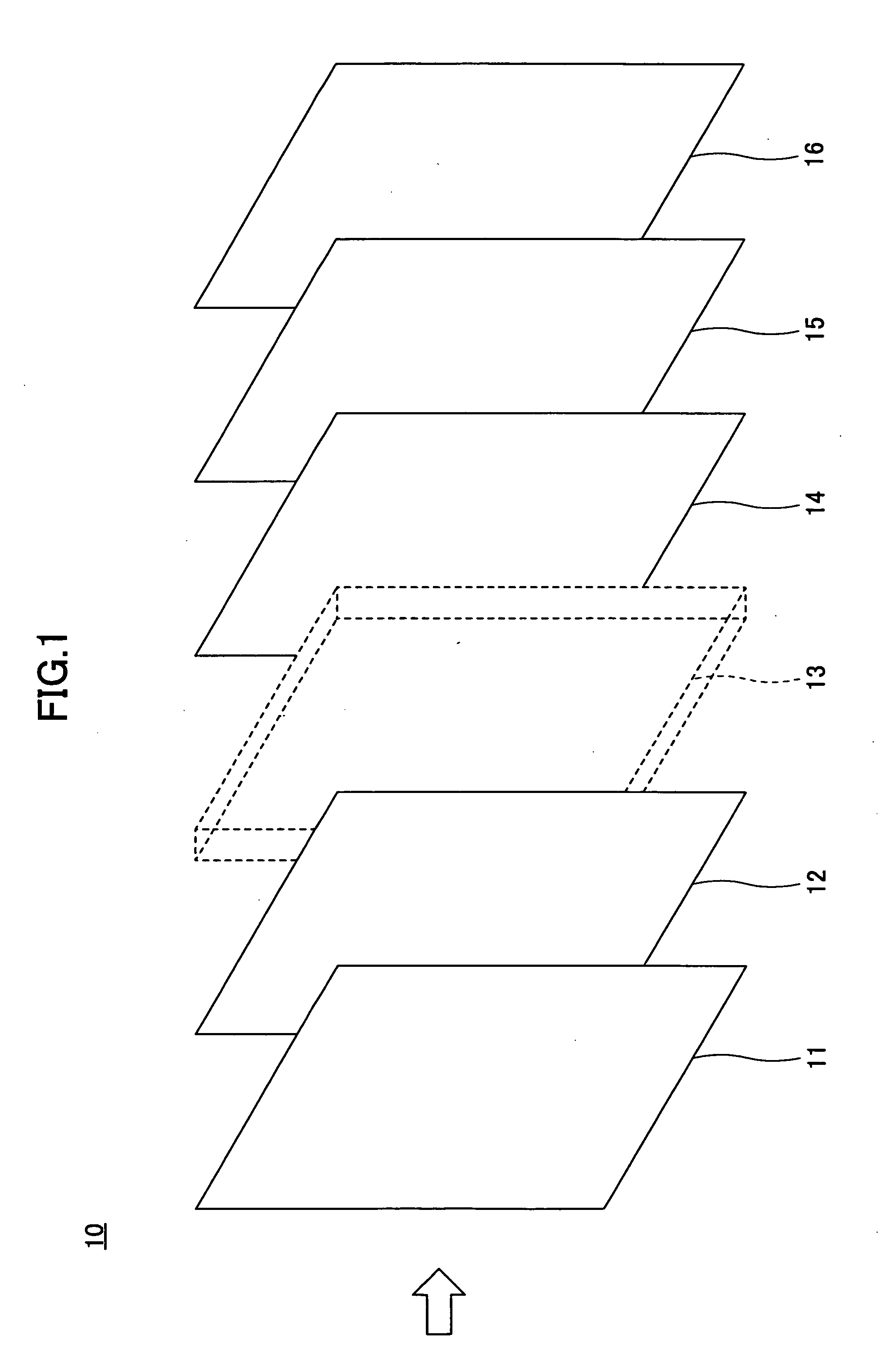
[0031]FIG. 1 is a schematic diagram showing a liquid crystal display (LCD) 10 according to a first embodiment of the present invention. In FIG. 1, the arrow indicates a viewing direction.
[0032] Referring to FIG. 1, the LCD 10 includes a polarizing plate 11, a color filter (CF) substrate 12 on which color filters are provided, a liquid crystal layer 13, a thin film transistor (TFT) substrate 14, a polarizing plate 15, and a backlight unit 16, which are stacked in this order from the viewing side.
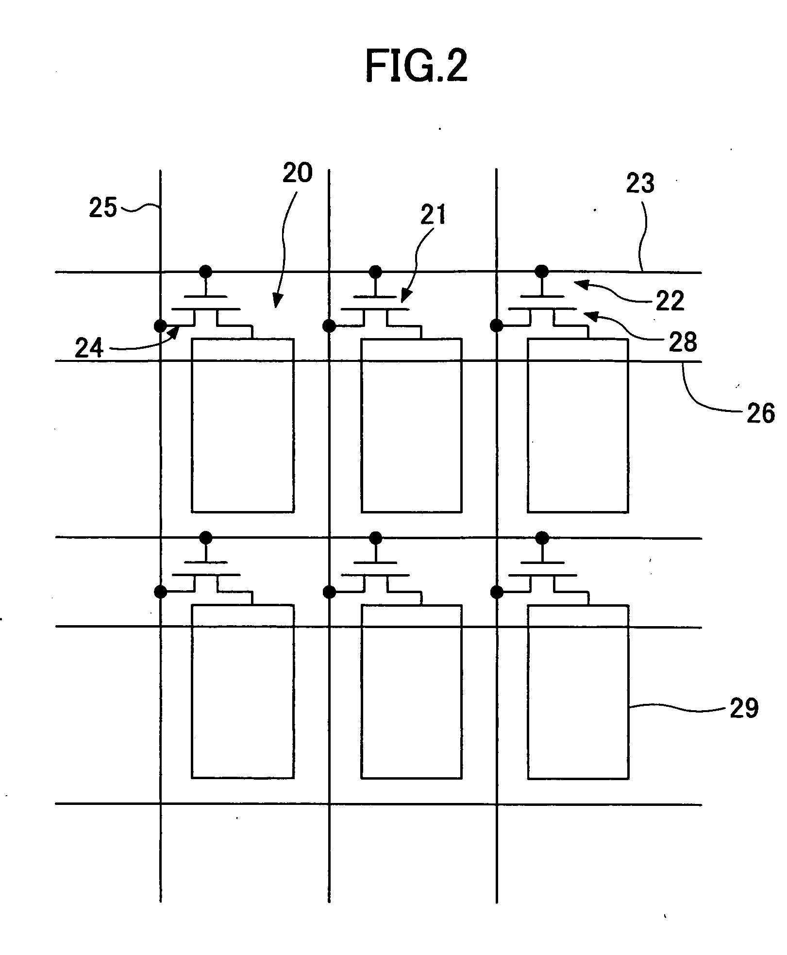
[0033]FIG. 2 is an equivalent circuit diagram of a pixel structure formed on the TFT substrate 14. Referring to FIG. 2, one TFT 21 is provided in each of pixel areas 20 disposed in a matrix manner. The gate of each TFT 21 extends laterally in FIG. 2, and is connected to a corresponding one of multiple gate bus lines 23 disposed parallel to one another. Further, a drain 24 of each TFT 21 extends vertically in FIG. 2, and is connected to a corresponding one of multiple drain bus lines 25 disp...
second embodiment
[0088] An LCD according to a second embodiment of the present invention, which is a variation of the LCD 10 of the first embodiment, is substantially the same as the LCD 10 except that the cross-sectional structures shown in FIGS. 6 and 8 are different in the LCD of the second embodiment. In the drawings, the elements corresponding to those described above are referred to by the same numerals, and a description thereof is omitted.
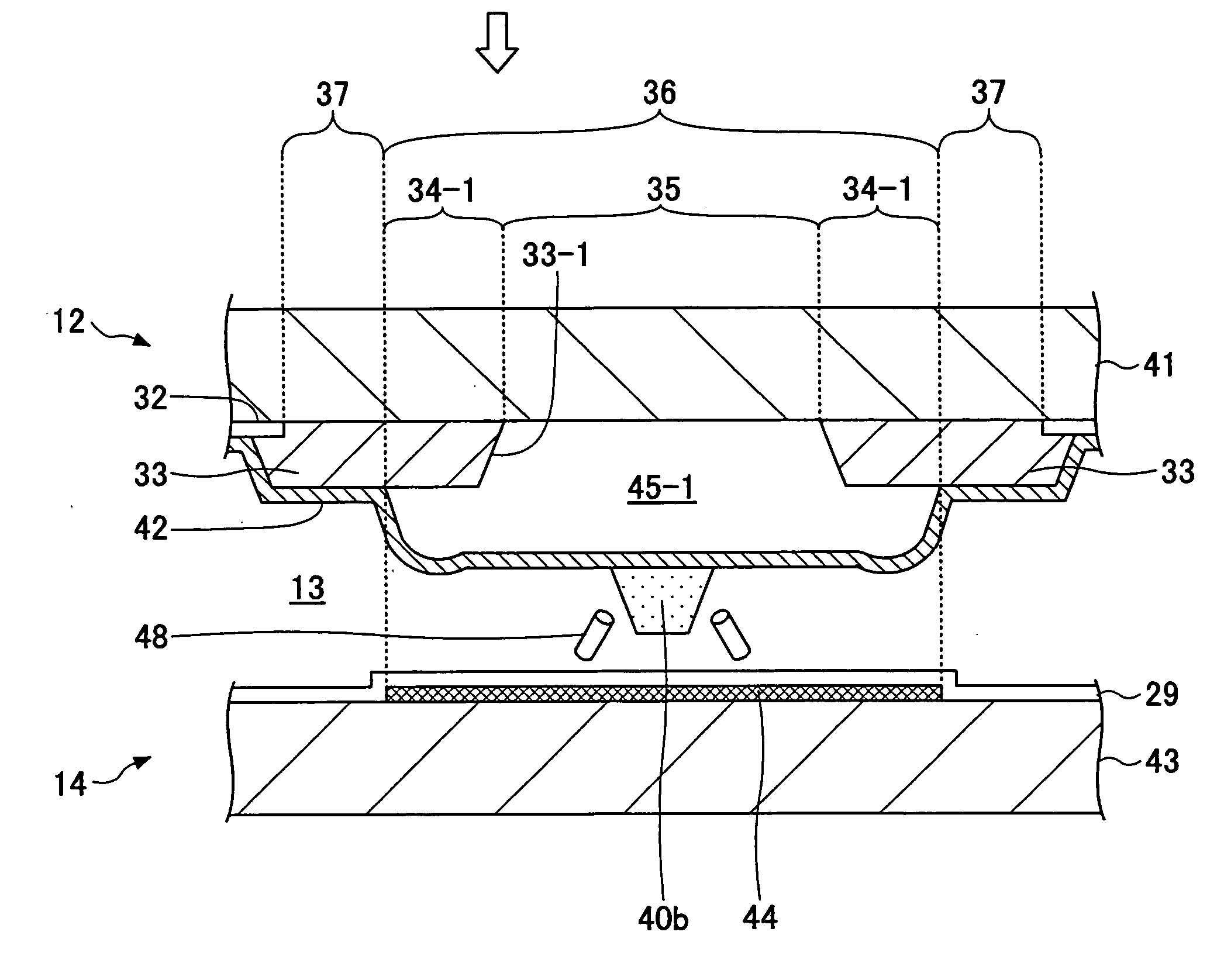
[0089]FIG. 12 is a cross-sectional view of part of a first pixel 60 of the LCD according to the second embodiment. FIG. 12 shows a cross-sectional view at the same position as the cross-sectional view taken along the line B-B of FIG. 4. Further, FIG. 13 is a cross-sectional view of part of a second pixel 70 of the LCD according to the second embodiment. FIG. 13 shows a cross-sectional view at the same position as the cross-sectional view taken along the line C-C of FIG. 7.
[0090] Referring to FIG. 12, the black matrix layer 32 and the color filter layer 33...
PUM
| Property | Measurement | Unit |
|---|---|---|
| height | aaaaa | aaaaa |
| thickness | aaaaa | aaaaa |
| thickness | aaaaa | aaaaa |
Abstract
Description
Claims
Application Information


