Organic electroluminescent display device

a technology of electroluminescent display and organic el, which is applied in the direction of static indicating devices, electroluminescent light sources, instruments, etc., can solve the problems of interrupting the miniaturization of the panel profile and the frame size is increased, so as to reduce the influence of voltage drop, increase the width of the power source bus line, and reduce the size of the picture frame

Active Publication Date: 2007-08-23
SAMSUNG DISPLAY CO LTD +1
View PDF5 Cites 7 Cited by
  • Summary
  • Abstract
  • Description
  • Claims
  • Application Information

AI Technical Summary

Benefits of technology

[0009]Accordingly, it is an object of the present invention to provide an organic EL display device which can decide respective line widths of power source lines which supply electricity to organic EL elements of respective colors corresponding to current quantities of the respective power source lines and can decrease a picture frame size thereof.
[0010]The present invention is directed to an organic EL display device which includes power source lines which are connected to a plurality of organic EL elements for respective colors and power source lines to which the power source lines are connected (hereinafter referred to as “power source bus lines”), and the power source bus line having a large current quantity is arranged on a side close to a display region for reducing the influence of a voltage drop attributed to the power source line.
[0011]Further, the present invention is characterized by increasing a width of the power source bus line with a large current quantity. Further, the power source bus line with a small current quantity is arranged outside the power source bus line with the large current quantity, and the power source line and the contact hole are connected with each other via a connection line made of a high-resistant material which is formed on a lower layer of the power source bus line.
[0012]As described above, according to the present invention, the widths of the power source bus lines for respective colors can be optimized within a range that the non-uniformity of the brightness in-plane distribution attributed to a voltage drop does not occur thus realizing the acquisition of an organic EL display device which can reduce a picture frame size while maintaining the display quality.

Problems solved by technology

Accordingly, a size of a so-called picture frame is increased thus interrupting the miniaturization of a profile of a panel.

Method used


Image

  • Organic electroluminescent display device
  • Organic electroluminescent display device
  • Organic electroluminescent display device

Examples


embodiment 1

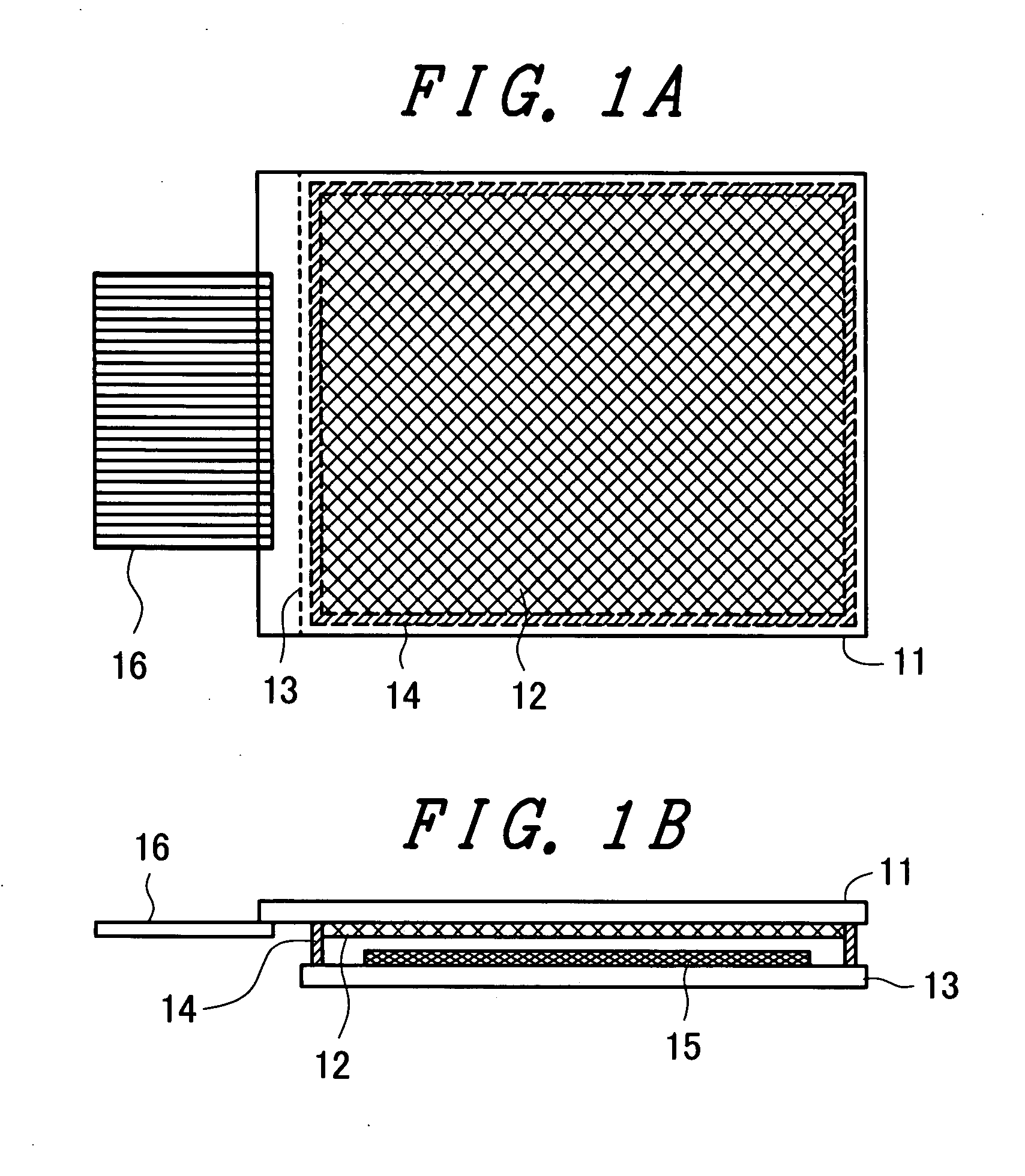
[0020]FIG. 1A and FIG. 1B are general appearance views of an organic EL display device according to the present invention, wherein FIG. 1A is a front view and FIG. 1B is a cross-sectional view. In FIG. 1A and FIG. 1B, a pixel part 12 is formed on a display substrate (display panel) 11, and the pixel part 12 is sealed by the display substrate 11, a sealing substrate 13 which faces the display substrate 11, and a sealing material 14. In a sealed space, for preventing the degradation of organic EL elements in the pixel part 12 due to moisture, a desiccant material 15 is sealed. Further, on the display substrate 11, an FPC (Flexible Printed Circuit) 16 for supplying signal for driving the organic EL elements and for supplying electricity from a power source part is mounted.

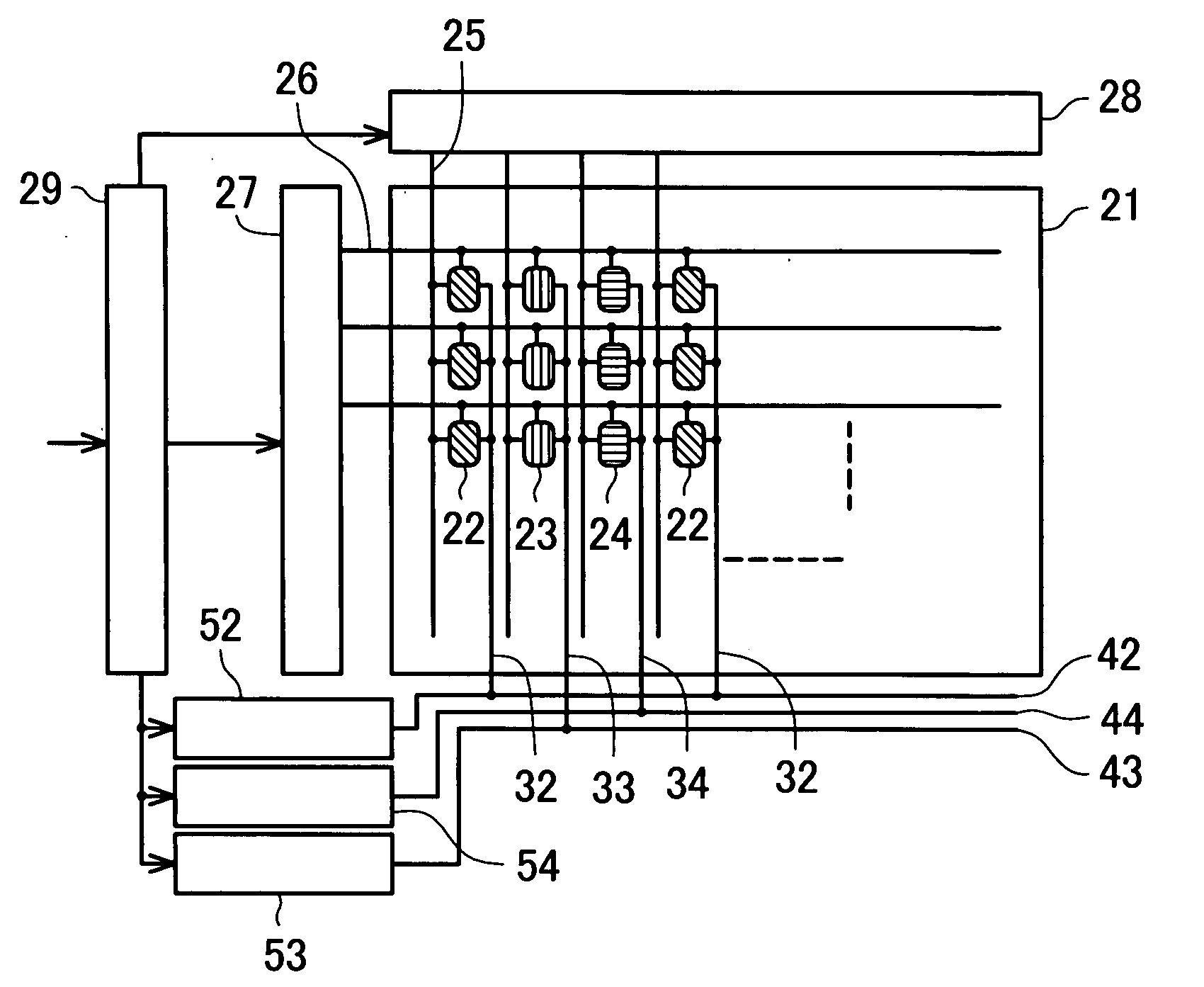
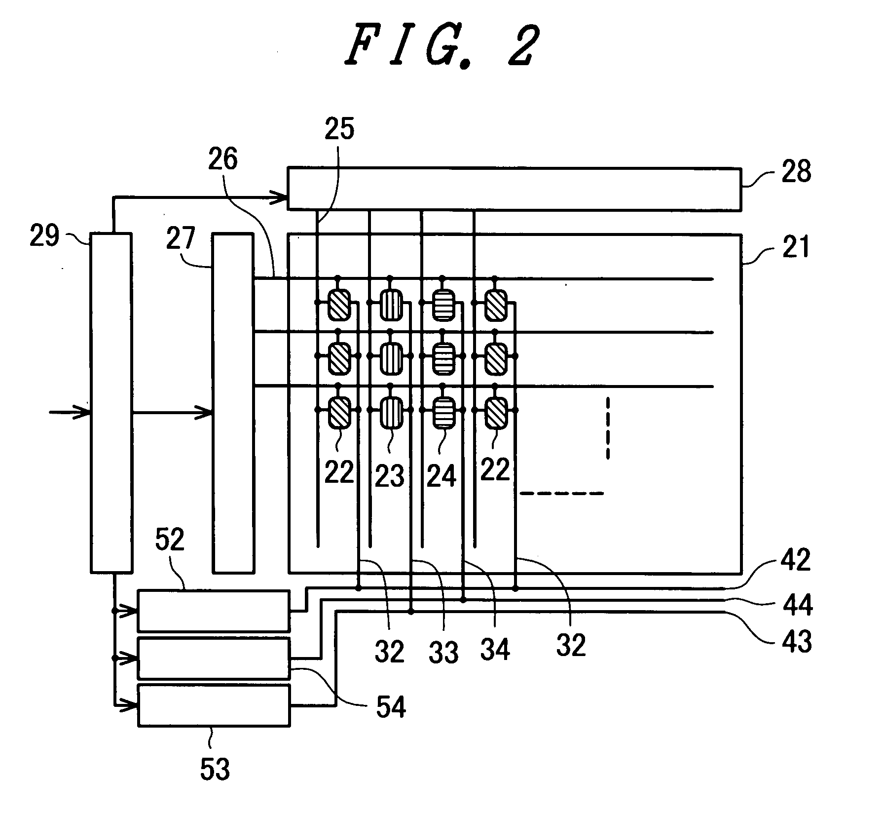
[0021]FIG. 2 is a drive circuit diagram of the organic EL display device shown in FIG. 1. In FIG. 1, for performing a full color display, within a display region 21, red pixels 22 which are constituted of an organic E...

embodiment 2

[0036]FIG. 6A to FIG. 6C are cross-sectional views of a connection between power source bus lines and a power source line, wherein FIG. 6A to FIG. 6C are respectively cross-sectional views of portions A, B and C in FIG. 5. In FIG. 6A to FIG. 6C, while respective power source lines 32, 33, 34 are made of Al (sheet resistance: 0.1 Ω / □), connection lines 83, 84 at line intersecting portions are made of MoW (sheet resistance: 1 Ω / □) which is a gate line material of a switching TFT.

[0037]The connection lines 83, 84 made of MoW are electrically connected to the power source lines 33, 34 made of Al in the same manner as power source bus lines 43, 44 made of Al via contact holes 82 formed in the insulation layer 81. In this case, since the resistance relationship is set as the resistance of MoW>>the resistance of Al and hence, assuming that the connection line is used as the power source bus line of a large current quantity, a voltage drop may become large. Further, even when the connection...


PUM


Abstract

The present invention narrows a picture frame size by deciding line widths of respective power source bus lines which supply electricity to organic EL elements of respective colors corresponding to current quantities of the respective power source bus lines. Red pixels, green pixels and blue pixels which are arranged in a matrix array and, and power source lines which are connected to the respective pixels are formed in a display region, and power source bus lines which supply electricity to these power source lines are formed in a picture frame region. The power source bus line for red of a large current quantity is arranged on a side close to the display region and the power source bus line for green of a small current quantity is arranged on an outer side.

Description

CROSS-REFERENCE TO RELATED APPLICATIONS [0001]The disclosure of Japanese Patent Application No. 2006-042310 filed on 2006 / 02 / 20 (yyyy / mm / dd) including the claims, the specification, the drawings and the abstract is incorporated herein by reference in its entirety.BACKGROUND [0002]1. Field of the invention[0003]The present invention relates to an organic EL display device which uses organic EL elements as pixels, and more particularly to an improved power source wiring which supplies electricity allowing the organic EL elements to emit light.[0004]2. Description of the Related Art[0005]An organic EL element is driven by an electric current and hence, it is necessary to eliminate the non-uniformity of the distribution of brightness in a display screen within a panel display region by arranging a bold power source line outside a panel display region thus suppressing a voltage drop of a power source. Accordingly, a size of a so-called picture frame is increased thus interrupting the min...

Claims


Application Information

Patent Timeline
Patent Type & Authority Applications(United States)
IPC IPC(8): G09G3/36
CPCH01L27/3279H01L27/3211H10K59/35H10K59/1315H05B33/26H05B33/02
Inventor FURUIE, MASAMITSUTOKUDA, NAOKI
Owner SAMSUNG DISPLAY CO LTD
Why Eureka
Try Eureka