Organic transistor and display device

a technology of organic transistors and display devices, which is applied in the direction of thermoelectric device junction materials, semiconductor devices, electrical apparatus, etc., can solve the problems of reducing the production process efficiency

Inactive Publication Date: 2007-05-03
RICOH KK
View PDF13 Cites 33 Cited by
  • Summary
  • Abstract
  • Description
  • Claims
  • Application Information

AI Technical Summary

Benefits of technology

[0025] According to one aspect of the present invention, there is provided an organic transistor including a stacked insulating film in which an insulating layer and a wettability control layer are stacked in order, whe

Problems solved by technology

As described above, after each thin film layer is formed, an active element can be fabricated by repeating the processes described above according to need, but expensive equipment and a long process line cause the cost to be higher.
Therefore, there is a possibility of realizing simplification or costing down of a production process.
However, since it is difficult to reduce the ejection quantity in ink jet printing, it is difficult to form a pattern equal to or less than 50 μm if the landing precision d

Method used


Image

  • Organic transistor and display device
  • Organic transistor and display device
  • Organic transistor and display device

Examples


embodiment (

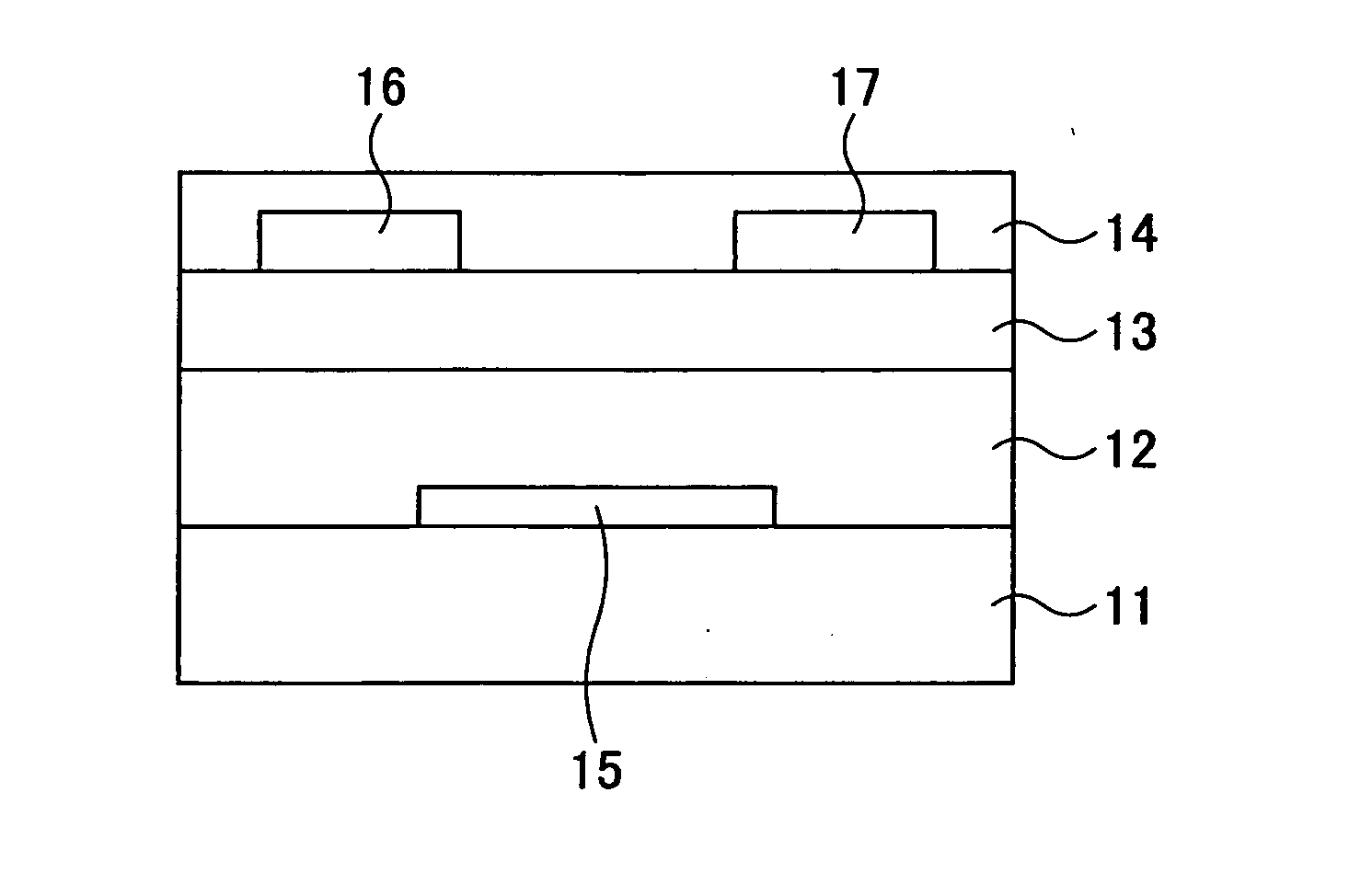
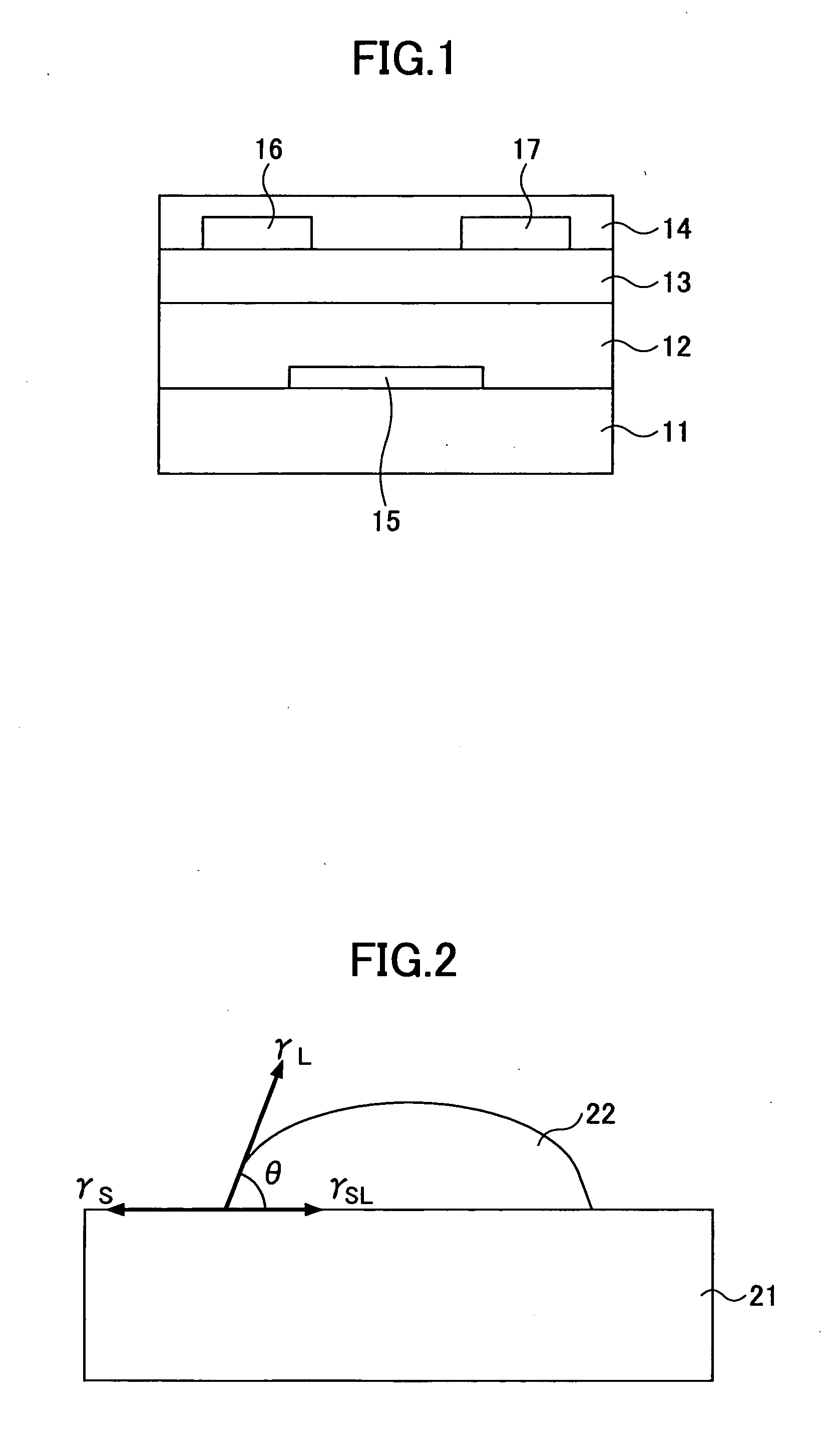
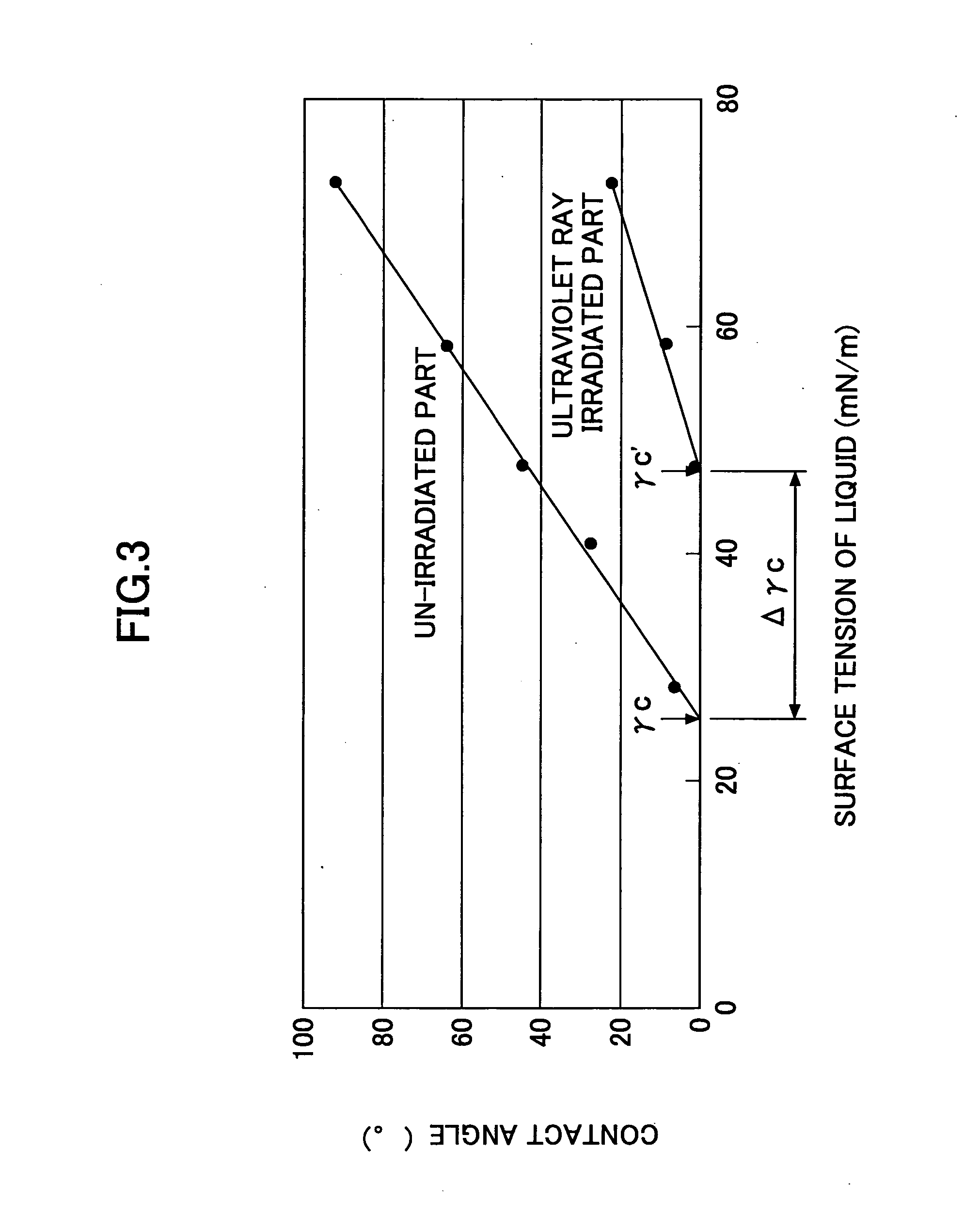
[0130] Embodiment (1) is an organic transistor having at least a stacked insulating film in which an insulating layer and a wettability control layer are stacked in order, characterized in that the wettability control layer contains a material whose surface energy can be changed by irradiation with an ultraviolet ray and a transmittance of the ultraviolet ray for irradiation therethrough is 10% or greater. 1), there can be provided an organic transistor in which the insulating property of a gate insulating film is good and which is capable of reducing electric power consumption.

[0131] Embodiment (2) is the organic transistor as described in embodiment (1) above, characterized in that a film thickness of the wettability control layer is 4 nm or greater and 200 nm or less. According to embodiment (2), an organic transistor in which the insulating property of a gate insulating film is good can be obtained.

[0132] Embodiment (3) is the organic transistor as described in embodiment (1) o...


PUM


Abstract

An organic transistor including a stacked insulating film in which an insulating layer and a wettability control layer are stacked in order is provided, wherein the wettability control layer includes a material whose surface energy can be changed by irradiation with an ultraviolet ray and a transmittance of the ultraviolet ray for irradiation therethrough is 10% or greater.

Description

BACKGROUND OF THE INVENTION [0001] 1. Field of the Invention [0002] The present invention relates to an organic transistor and a display device. [0003] 2. Description of the Related Art [0004] Recently, an organic thin-film transistor using an organic semiconductor material has been actively studied. As an advantage of an organic thin-film transistor, for example, the flexibility thereof, sizing up of the surface area thereof, simplification of a production process due to a simple layer structure thereof, and cost down of a production apparatus therefore can be listed. As a result, production thereof which is less expensive than that of a conventional Si-based semiconductor device can be provided. Further, a thin film or a circuit can be easily formed by, for example, a printing method, a spin-coat method, and a dipping method. [0005] As one parameter for indicating the characteristic of an organic thin-film transistor, an on / off ratio (Ion / Ioff) of electric current is provided. In ...

Claims


Application Information

Patent Timeline
IPC IPC(8): H01L29/08
CPCH01L51/0533H10K10/476
Inventor TANO, TAKANORISUZUKI, KOEIKAWASHIMA, IKUEAKIYAMA, YOSHIKAZU
Owner RICOH KK
Why Eureka
Try Eureka