Switchable PLL circuit

a technology of switching circuit and pll circuit, which is applied in the direction of electrical apparatus, pulse automatic control, etc., can solve the problems of less stable frequency and phase vcxos, and the output signal of a pll circuit using vcxos may have a higher amount of clock jitter, so as to achieve a large locking range, low jitter, and high jitter

Active Publication Date: 2007-05-10
INTERDIGITAL MADISON PATENT HLDG
View PDF6 Cites 17 Cited by
  • Summary
  • Abstract
  • Description
  • Claims
  • Application Information

AI Technical Summary

Benefits of technology

[0004] It is, therefore, desirable to have a circuit that provides locking to an input signal, producing an output clock signal with low jitter while at the same time exhibiting a large locking range.
[0005] The invention suggests combining two PLL circuits having individual control stages, wherein one of the PLL circuits uses a TCXO and the other one uses a VCXO as an oscillator. The two PLL circuits are either used individually or in a cascaded manner, depending on the operating mode.
[0006] In a first operating mode the two PLL circuits are connected in a first configuration that provides a larger locking range. To this end the input signal is supplied to both, the first and the second PLL circuit. The first PLL circuit has a controllable oscillator that has a relatively small pulling range and attempts to lock onto the input signal in the known way. Controllable oscillators having a relatively small pulling range but good phase frequency and temperature stability are, for example, temperature controlled crystal oscillators, or TCXOs. The controllable oscillator of the first PLL circuit has, however, the capability of oscillating with a nominal frequency in case of the absence of an input signal. In this case the first oscillator acts as a clock master which provides an excellent jitter quality. Further, the controllable oscillator of the first PLL circuit has a very stable phase and frequency behaviour. The second PLL circuit has a controllable oscillator which has a relatively large pulling range compared to the controllable oscillator of the first PLL circuit. The controllable oscillator of the second PLL circuit is, for example, a voltage controlled crystal oscillator, or VCXO. In the following specification the terms VCXO and TCXO are used as synonyms for controllable oscillators having a large as a small pulling range, respectively. The second PLL circuit thus has a large a locking range. In this first operating mode it also attempts to lock onto the input signal. As the second PLL circuit has a larger locking range it is very likely that it will lock onto the input signal at first. A lock detector provides information about the locking state of the first PLL circuit which has a smaller locking range than the second PLL. When the first PLL circuit is locked on to the input signal the two PLL circuits are connected in a second configuration that provides improved jitter behaviour compared to the first configuration, while having a smaller locking range. This operating mode is also referred to in the following as a second operating mode. Whenever the lock detector determines that the first PLL circuit is not locked the two PLL circuits are again connected in the first configuration. In case no input signal is present at all the TCXO oscillator of the first PLL circuit is oscillating freely at its nominal frequency. The output signal of the first PLL circuit is then supplied to the second PLL circuit, which locks onto the output signal of the first PLL circuit. This operating mode is also referred to in the following as a third operating mode.

Problems solved by technology

VCXOs, however, are less stable in frequency and phase compared to TCXOs and thus the output signal of a PLL circuit using VCXOs may have a higher amount of clock jitter compared to a PLL circuit using a TCXO.

Method used


Image

  • Switchable PLL circuit
  • Switchable PLL circuit
  • Switchable PLL circuit

Examples


Embodiment Construction

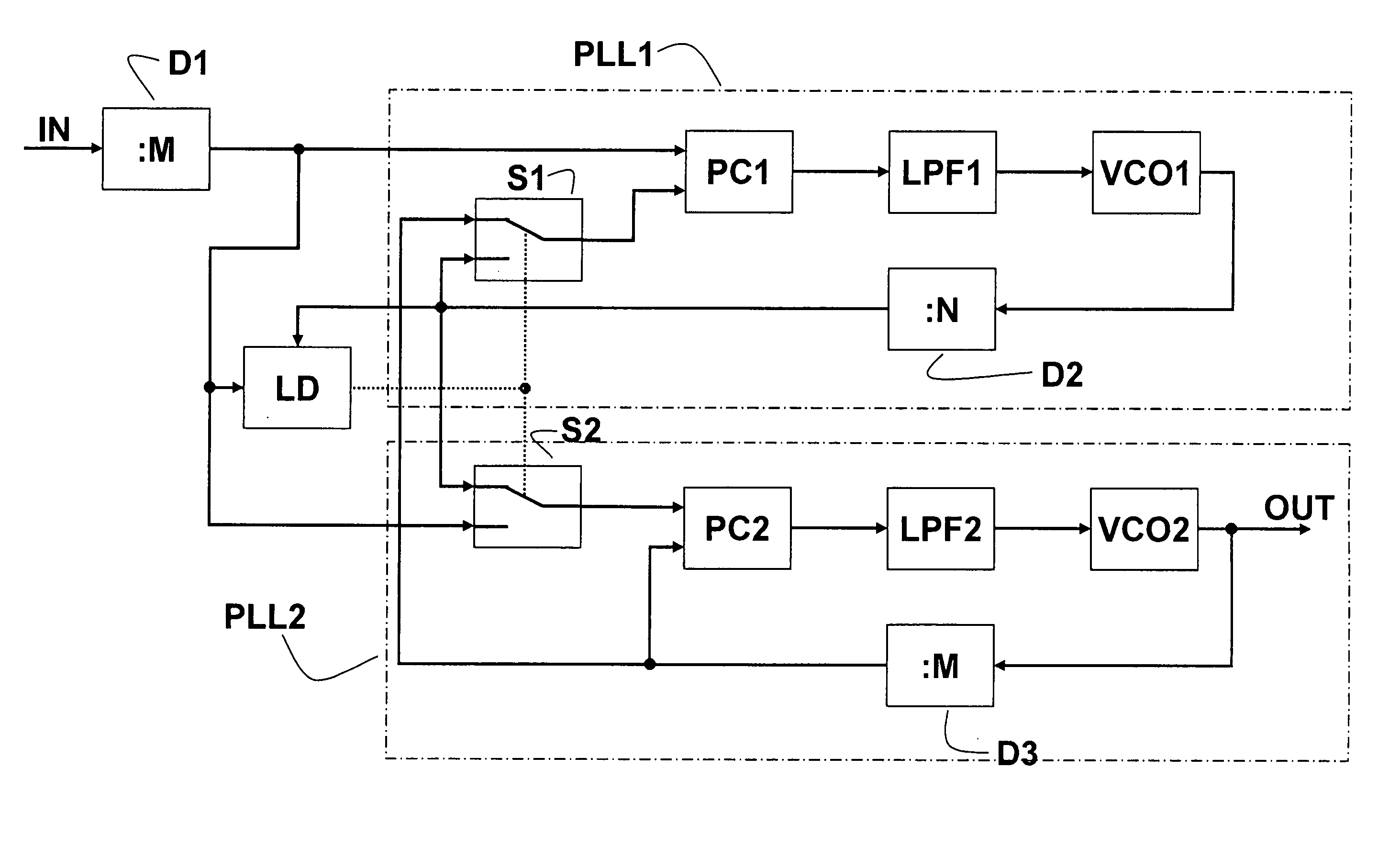
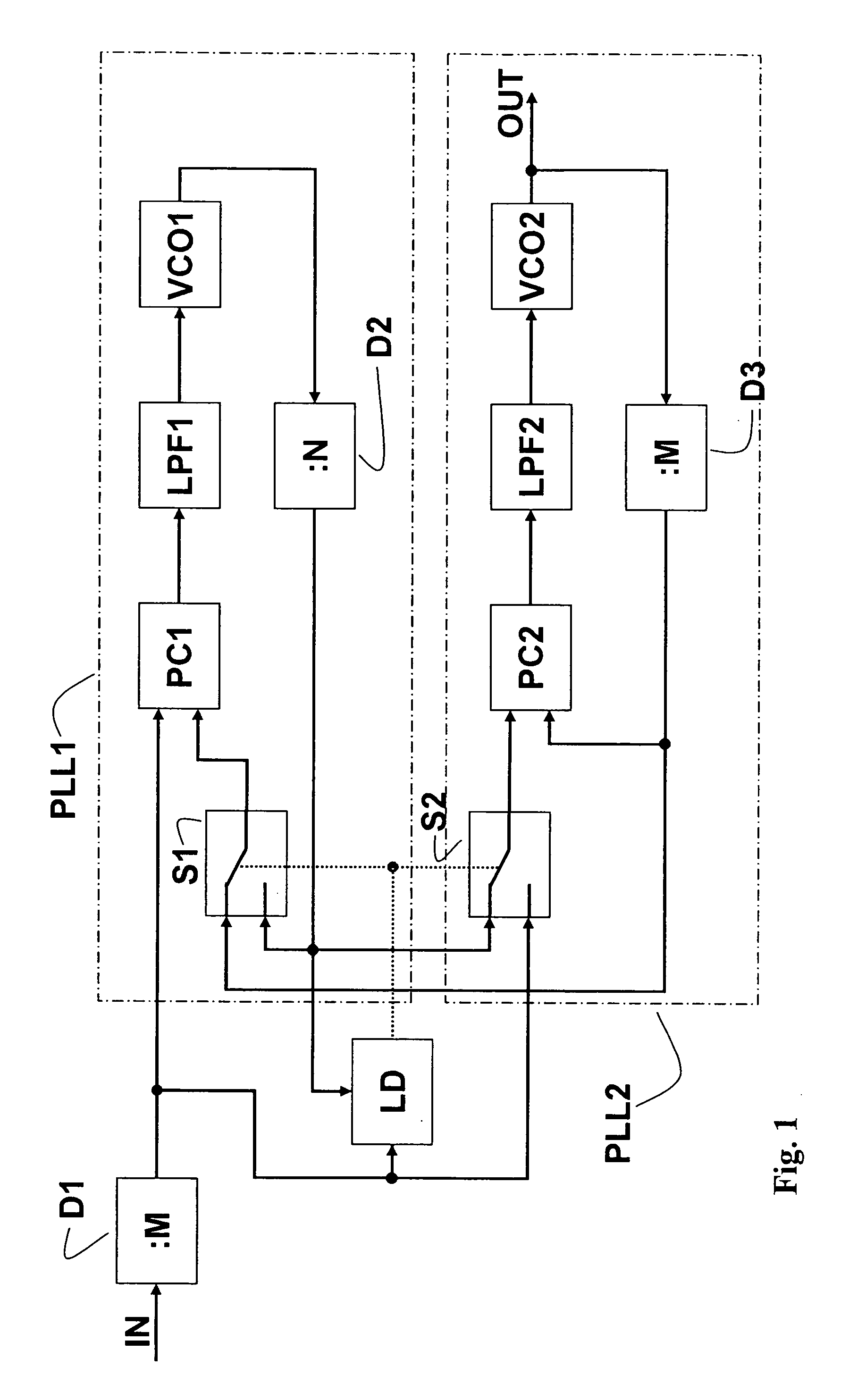
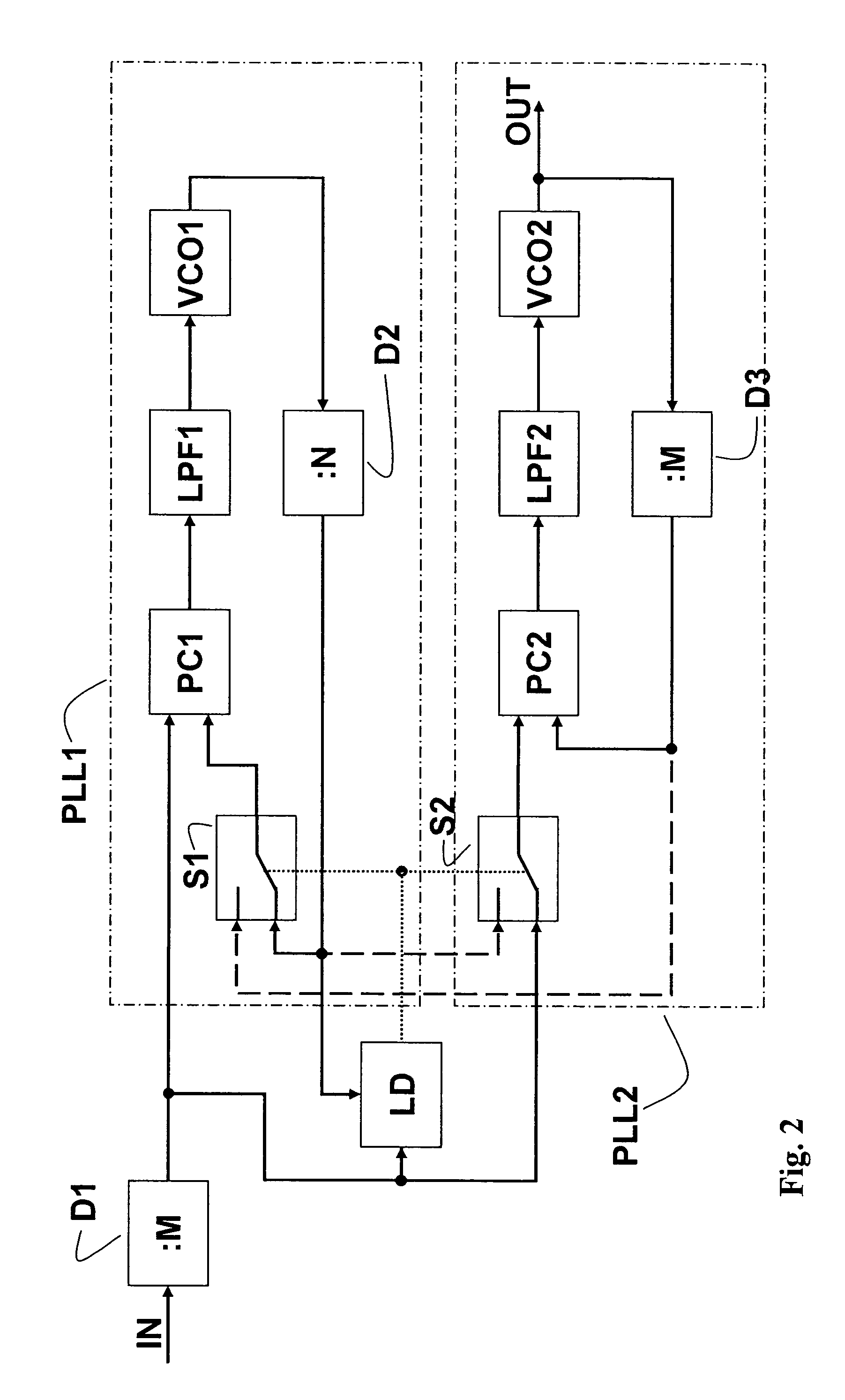
[0013] In FIG. 1 a block diagram of the inventive circuit is shown. An input signal IN is supplied via a first divider D1 to a first input of a first phase comparator PC1 of a first PLL circuit PLL1. To a second input of the first phase comparator PC1 an output signal of a first controllable oscillator VCO1 is supplied via a second divider D2 and a first switch S1. The first controllable oscillator VCO1 is controlled by the output signal of the first phase comparator PC1 which is supplied to the first controllable oscillator VCO1 via a first filter LPF1. The output signal of the first controllable oscillator VCO1 is further supplied to a lock detector LD, which also receives the input signal IN after division in the first divider D1. The lock detector LD controls the first switch S1, which selectively applies the output signal of the first controllable oscillator VCO1 or the output signal of a second controllable oscillator VCO2 to the second input of the first phase comparator PC1....


PUM


Abstract

An electronic circuit includes a first and a second PLL stage (PLL1, PLL2) that can be switched in parallel or in series depending on locking of the first one of the PLL circuits to an input signal (IN). When in parallel, only the second PLL circuit (PLL2) is actively supplying a clock signal to the output of the electronic circuit. The first PLL circuit (PLL1) continues trying to lock onto the input signal (IN). A lock detector (LD) monitors the locking status of the first PLL circuit (PLL1) to the input signal (IN) and, upon locking, sets switches (S1, S2) to couple the output of the first PLL circuit (PLL1) to the input of the second PLL circuit (PLL2), and to couple the output of the second PLL circuit (PLL2) to the input of the first PLL circuit (PLL1).

Description

FIELD OF THE INVENTION [0001] The invention relates to an electronic circuit including two PLL circuits which can be switched between different configurations. In particular, the invention relates to PLL circuits in which controlled oscillators have to be locked with respect to frequency and phase to an input clock. BACKGROUND OF THE INVENTION [0002] This section is intended to introduce the reader to various aspects of art, which may be related to various aspects of the present invention that are described and / or claimed below. This discussion is believed to be helpful in providing the reader with background information to facilitate a better understanding of the various aspects of the present invention. Accordingly, it should be understood that these statements are to be read in this light, and not as admissions of prior art. [0003] Electronic circuits which are supplied an input signal at a certain clock frequency often need to process the received input signal in further process...

Claims


Application Information

Patent Timeline
Patent Type & Authority Applications(United States)
IPC IPC(8): H03L7/06
CPCH03L7/07H03L7/143H03L7/22H03L7/087
Inventor DREXLER, MICHAELSCHAEFER, RALF-DETLEF
Owner INTERDIGITAL MADISON PATENT HLDG
Why Eureka
Try Eureka