Gate critical dimension variation by use of ghost features
- Summary
- Abstract
- Description
- Claims
- Application Information
AI Technical Summary
Problems solved by technology
Method used
Image

Examples
Embodiment Construction
[0001] 1. Field of the Invention
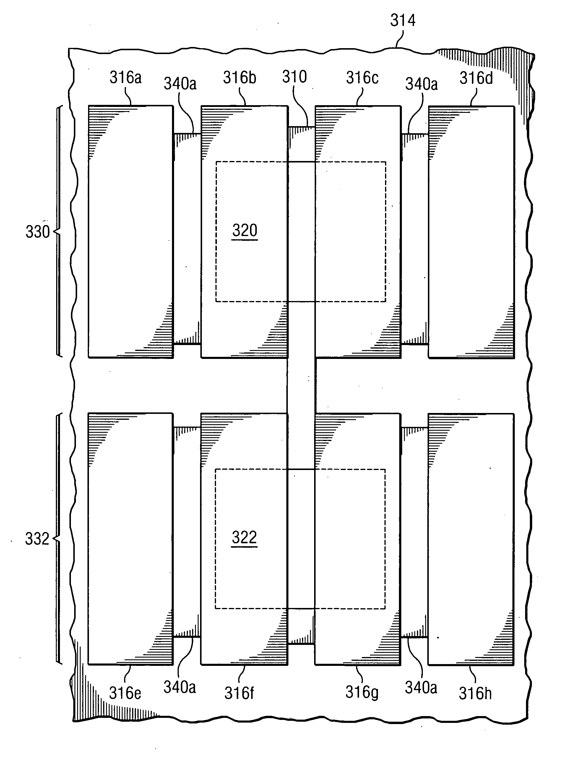
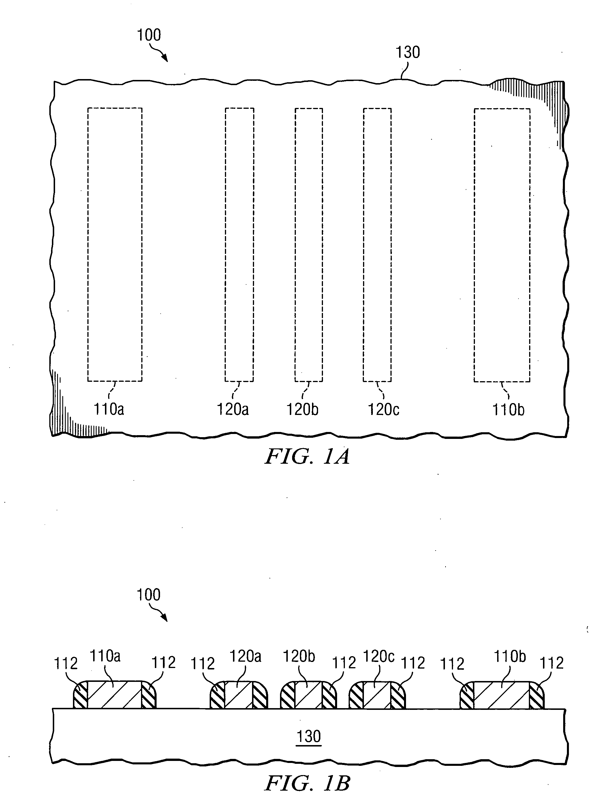
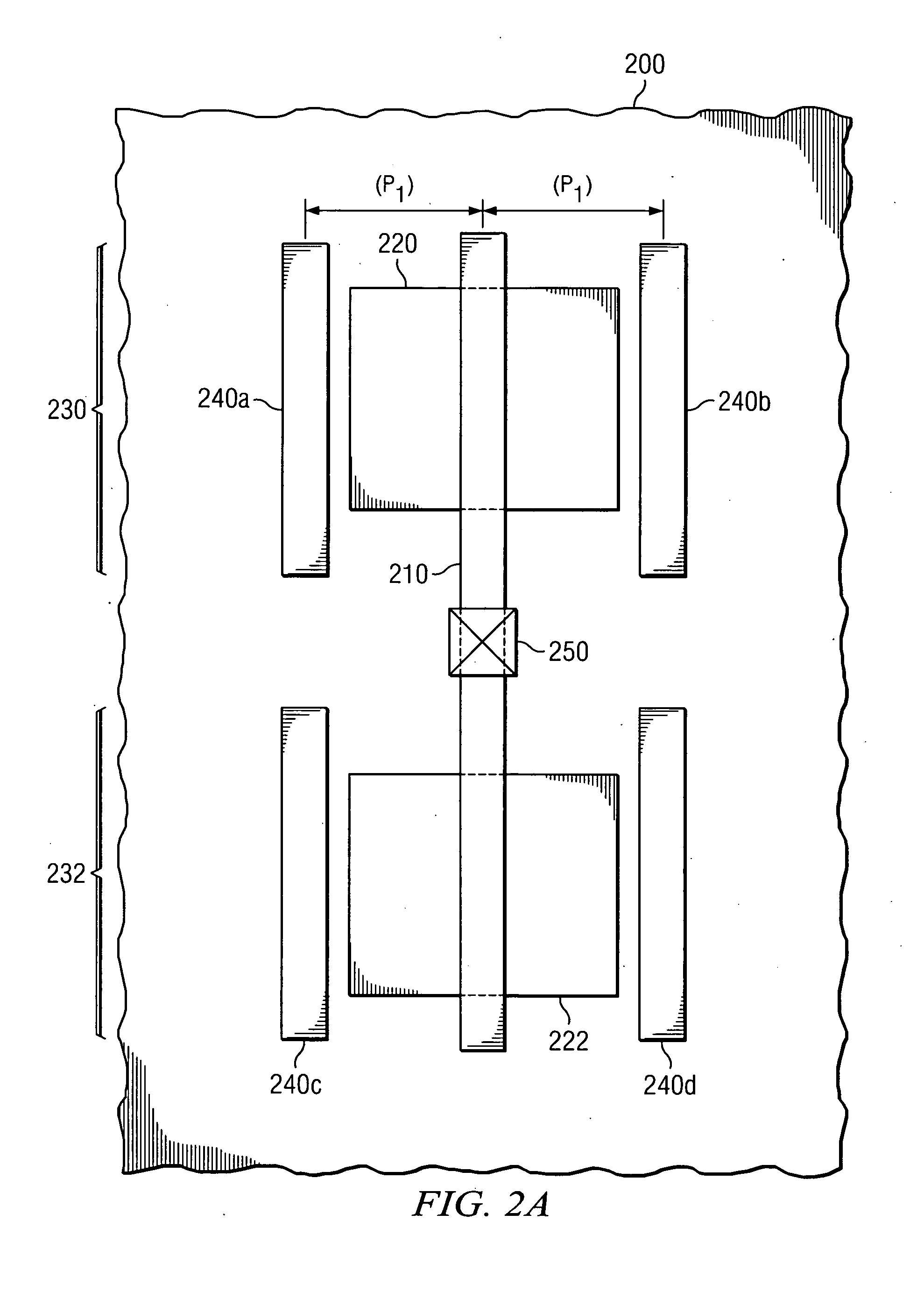
[0002] The subject matter of this invention relates to photolithography for forming integrated circuit devices. More particularly, the subject matter of this application relates to methods and devices used to improve gate critical dimension variation.
[0003] 2. Background of the Invention
[0004] Lithographic projection apparatus (tools) can be used, for example, in the manufacture of integrated circuits (ICs). When using the various tools, a mask can be used that contains a circuit pattern corresponding to an individual layer of the IC, and this pattern, usually having many designs, can be imaged onto a target portion (e.g., comprising one or more dies) on a substrate, such as a silicon or other wafer comprising a semiconductor, that has been coated with a layer of radiation-sensitive material, such as a resist. In general, a single wafer may contain a network of adjacent target portions that can be successively irradiated using a projection system o...
PUM
 Abstract
Description
Claims
Application Information
 - R&D Engineer
- R&D Manager
- IP Professional
- Industry Leading Data Capabilities
- Powerful AI technology
- Patent DNA Extraction
Browse by: Latest US Patents, China's latest patents, Technical Efficacy Thesaurus, Application Domain, Technology Topic.
© 2024 PatSnap. All rights reserved.Legal|Privacy policy|Modern Slavery Act Transparency Statement|Sitemap