
Photoelectric conversion device for reducing radiation noise on large screen sensors

a technology of radiation noise reduction and conversion device, which is applied in the field of photoelectric conversion device, can solve the problems of degrading the reliability of the photoelectric conversion device, unable to perfect eliminate fine dust during the fabrication of the photoelectric conversion semiconductor layer, and unable to achieve the effect of preventing the effect of radiation nois

Inactive Publication Date: 2007-05-17
CANON KK
View PDF30 Cites 1 Cited by
  • Summary
  • Abstract
  • Description
  • Claims
  • Application Information

AI Technical Summary

Benefits of technology

[0017] The present invention has been accomplished in view of the above problems and an object of the present invention is to provide a photoelectric conversion device that can surely prevent the effect of radiation noise on the large-screen sensor such as the contact type sensor having mounted photoelectric conversion elements as two-dimensionally arrayed at equal intervals, by a low-cost and simple mounting structure without depositing films.
[0018] Another object of the present invention is to provide a photoelectric conversion device with a high SN ratio and also to provide a photoelectric conversion device with excellent environment resistance.
[0019] A further object of the present invention is to provide a photoelectric conversion device that can prevent deterioration of the wavelength converting member such as the fluorescent member, due to humidity, water, or the like, thereby permitting stable reading.
[0021] In the present invention, by providing by sticking on a photoelectric conversion element comprising a semiconductor material capable of photoelectric conversion or the like as a component, a conductive member having at least a conductive layer such as a thin metal sheet (of course, the conductive member may have only the conductive layer), the above-mentioned problems can be solved to provide a photoelectric conversion device with a sufficiently high SN ratio, high reliability, and sufficient durability.
[0022] Since the present invention involves no need for an advanced process during the step of providing the conductive material, the invention can provide a more inexpensive photoelectric conversion device with high cost performance and in a higher yield.

Problems solved by technology

In such large-screen sensors with high characteristics, however, because of their large screen and large area, there were some cases where increase in radiation noise caused noise voltage or noise current to enter the photoelectric conversion semiconductor layers and the TFT semiconductor layers and to cause an error operation or an error signal, thereby extremely degrading the reliability of the photoelectric conversion device.
It is, however, undeniable that the metal film formed by vacuum vapor deposition or the like is disadvantageous in terms of the cost.
Further, it is impossible to perfectly eliminate fine dust during fabrication of the photoelectric conversion semiconductor layers, particularly two types of dust that poses a problem; dust particles peeled off from the inner wall of a thin-film deposition apparatus during deposition of an amorphous silicon layer on the substrate; and dust particles remaining on a substrate during deposition of a metal layer on the substrate.
In addition to the circumstance that it was originally impossible to perfectly eliminate the defective condition of wire, i.e., short or open of wire, there arises the problem that the method for forming the metal film by vacuum vapor deposition or the like, and patterning it to effect wiring in order to form the antenna earth for preventing the radiation noise from entering the device would be a factor that further lowers the yield of the substrates and raises the cost in production of a large-screen photoelectric conversion device.
This, however, forces more difficult formation of films and thus does not substantially solve the above problem.
From another aspect, the wavelength converting member such as the fluorescent screen is often rather vulnerable to an external factor such as humidity.

Method used


Image

  • Photoelectric conversion device for reducing radiation noise on large screen sensors
  • Photoelectric conversion device for reducing radiation noise on large screen sensors
  • Photoelectric conversion device for reducing radiation noise on large screen sensors

Examples


Embodiment Construction

[0052] The present invention will be described by reference to the accompanying drawings as occasion may demand.

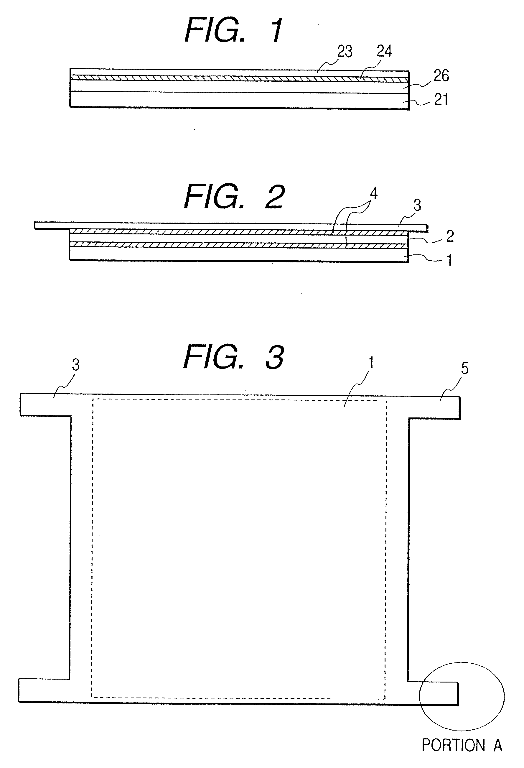
[0053]FIG. 2 is a schematic, cross-sectional view of an example of a photoelectric conversion device capable of reading an X-ray image, in which an X-ray image on a fluorescent member radiating light with reception of X-rays traveling through an object is electrically read by a photoelectric conversion element.

[0054] The photoelectric conversion device of the present invention generally concerns the contact sensors of the 1:1 reading type with a photoelectric conversion layer comprising a material capable of photoelectric conversion such as a-Si, particularly all two-dimensional sensors, but the device will be described with typical examples of application as image information reading means of the X-ray roentgen apparatus (X-ray imaging apparatus).

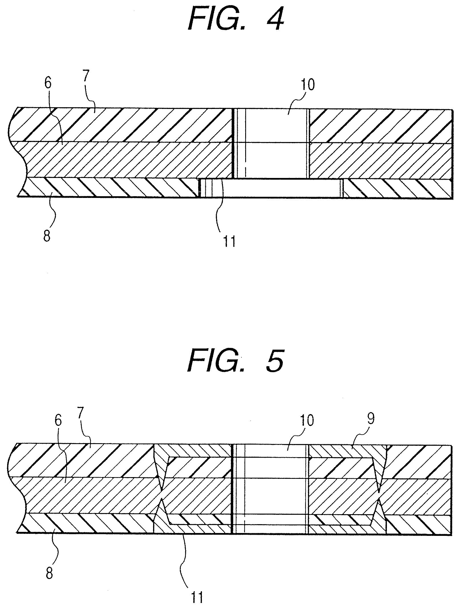
[0055]FIG. 2 shows an example of a photoelectric conversion device in which a fluorescent screen 2 for converting X-rays int...


PUM


Abstract

For providing a photoelectric conversion device that can prevent radiation noise by a low-cost and simple mounting method, the photoelectric conversion device having a photoelectric conversion element is provided in which a conductive member such as a thin metal sheet is stuck on the photoelectric conversion element.

Description

BACKGROUND OF THE INVENTION [0001] 1. Field of the Invention [0002] The present invention relates to a photoelectric conversion device, and more particularly, relates to a photoelectric conversion device having a two-dimensional photoelectric conversion region suitably used for reading (particularly, for reading with 1:1 magnification), for example, in facsimile machines, digital copiers, X-ray imaging apparatuses for nondestructive inspection, or the like. [0003] 2. Related Background Art [0004] There are conventionally known those reading devices which use a reducing (demagnifying) optical system and a CCD type sensor as image reading devices for facsimile machines, copiers, scanners, or X-ray imaging apparatuses (so-called roentgen apparatus). With the development of photoelectric conversion semiconductor materials typified by hydrogenated amorphous silicon (hereinafter referred to as a-Si), development is remarkable of so-called contact type sensors in which a photoelectric conv...

Claims


Application Information

Patent Timeline
Patent Type & Authority Applications(United States)
IPC IPC(8): H01L31/00H01L27/14G01T1/20G01T1/24H01L31/02H01L31/0203H01L31/0232H01L31/04H01L31/09H04N1/028H04N5/335H04N5/357H04N5/369H04N5/374H04N5/378
CPCH01L27/14618H01L27/14663H01L27/14683H01L31/02322Y02B10/14H01L2924/0002Y02B10/10H01L2924/00G01T1/20H01L31/02
Inventor TAKAMI, EIICHIKAIFU, NORIYUKIKAJIWARA, KENJI
Owner CANON KK
Learn More