Volatile memory elements with boosted output voltages for programmable logic device integrated circuits

a technology of integrated circuits and memory elements, which is applied in the direction of power supply for data processing, instruments, measurement devices, etc., can solve the problems of excessive voltage loss of data signals passing through the pass transistor, no longer being recognizable as valid logic signals on the device, and only working properly of the pass transistor, etc., to achieve the effect of increasing the write margin of memory elements and reducing the power supply voltage used to power the memory elements

Active Publication Date: 2007-05-17
ALTERA CORP
View PDF19 Cites 25 Cited by
  • Summary
  • Abstract
  • Description
  • Claims
  • Application Information

AI Technical Summary

Benefits of technology

[0011] The memory elements are loaded with configuration data using data lines. Address lines and address transistors are used to control which memory elements are loaded. The power supply voltage that is used to power the memory elements is reduced during data loading operations. This increases the write margin for the memory elements while relaxing requirements for the address transistors.

Problems solved by technology

The pass transistors in a programmable logic device will only operate properly if they are driven at a large enough voltage.
If the pass transistors in a programmable logic device are driven at an insufficient voltage level because, for example, the Vcc level on the device is too low, the data signals passing through the pass transistors will suffer excessive voltage loss and may no longer be recognizable as valid logic signals on the device.

Method used


Image

  • Volatile memory elements with boosted output voltages for programmable logic device integrated circuits
  • Volatile memory elements with boosted output voltages for programmable logic device integrated circuits
  • Volatile memory elements with boosted output voltages for programmable logic device integrated circuits

Examples


Embodiment Construction

[0024] The present invention relates to integrated circuits that contain memory elements. The invention also relates to memory elements and circuits for loading data into the memory elements. The integrated circuits may be memory chips, digital signal processing circuits with memory arrays, microprocessors, application specific integrated circuits with memory arrays, programmable logic device integrated circuits in which memory elements are used for configuration memory, or any other suitable integrated circuit. For clarity, the present invention will generally be described in the context of programmable logic device integrated circuits and programmable logic device memory elements.

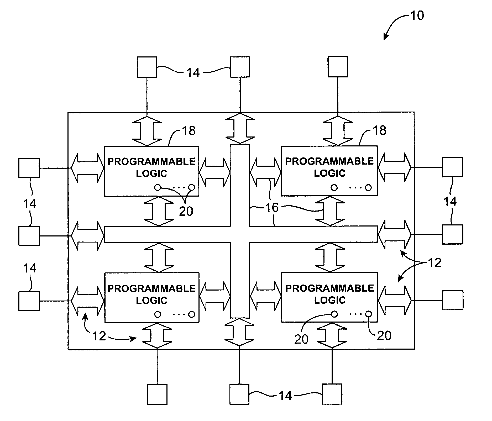
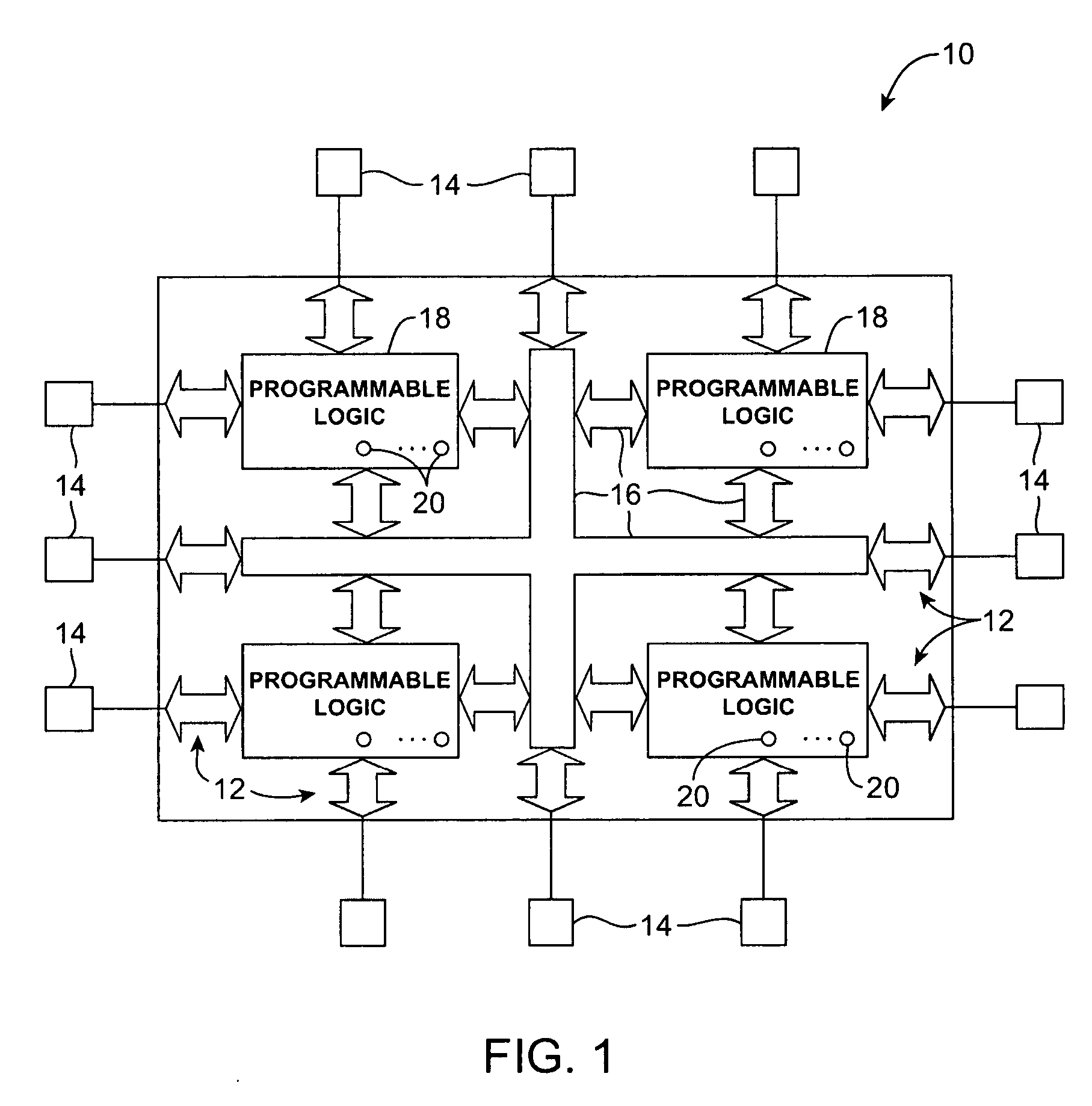
[0025] An illustrative programmable logic device 10 in accordance with the present invention is shown in FIG. 1.

[0026] Programmable logic device 10 may have input / output circuitry 12 for driving signals off of device 10 and for receiving signals from other devices via input / output pins 14. Interconnecti...


PUM


Abstract

Integrated circuits are provided that have memory elements. The memory elements produce output signals. The integrated circuits may be programmable logic device integrated circuits containing programmable logic including transistors with gates. When loaded with configuration data, the memory elements produce output signals that are applied to the gates of the transistors in the programmable logic device to customize the programmable logic. To ensure that the transistors in the programmable logic are turned on properly, the memory elements are powered with an elevated power supply level during normal device operation. During data loading operations, the power supply level for the memory elements is reduced. Reducing the memory element power supply level during loading increases the write margin for the memory elements.

Description

BACKGROUND [0001] This invention relates to volatile memory elements, and more particularly, to volatile memory elements that have elevated output voltages for integrated circuits such as programmable logic devices. [0002] Integrated circuits often contain volatile memory elements. Typical volatile memory elements are based on cross-coupled inverters (latches) and are used to store data. Each memory element can store a single bit of data. [0003] Volatile memory elements are often used to store configuration data in programmable logic devices. Programmable logic devices are a type of integrated circuit that can be customized in relatively small batches to implement a desired logic design. In a typical scenario, a programmable logic device manufacturer designs and manufactures uncustomized programmable logic device integrated circuits in advance. Later, a logic designer uses a logic design system to design a custom logic circuit. The logic design system uses information on the hardwar...

Claims


Application Information

Patent Timeline
Patent Type & Authority Applications(United States)
IPC IPC(8): G06F1/26
CPCG06F1/3225
Inventor LIU, LIN-SHIHCHAN, MARK T.
Owner ALTERA CORP
Why Eureka
Try Eureka