Display device and manufacturing method

a technology of a display device and a manufacturing method, which is applied in the direction of thermoelectric devices, electroluminescent light sources, electric lighting sources, etc., can solve the problems of difficult to properly control the nozzle used to jet organic semiconductor solutions and uniform characteristics of organic semiconductors, and achieve the effect of improving the processing margin of ink-jet printing processes

Inactive Publication Date: 2007-05-24
SAMSUNG ELECTRONICS CO LTD
View PDF0 Cites 7 Cited by
  • Summary
  • Abstract
  • Description
  • Claims
  • Application Information

AI Technical Summary

Benefits of technology

[0011] Accordingly, it is an aspect of the present invention to provide a display device in which the processing margin of the ink-jet printing process is improved.
[0012] Another aspect of the present invention is to provide a manufacturing method of a display device which improves the processing margin of the ink-jet printing process.

Problems solved by technology

However, it is difficult to properly control the nozzle used to jet the organic semiconductor solution to the enclosed areas for the TFTs, since the areas are very small.
Thus, the organic semiconductor layer may not be patterned to a desired shape, or its thickness may be different for different pixels, so that characteristics of the organic semiconductor are not uniform.

Method used


Image

  • Display device and manufacturing method
  • Display device and manufacturing method
  • Display device and manufacturing method

Examples


first embodiment

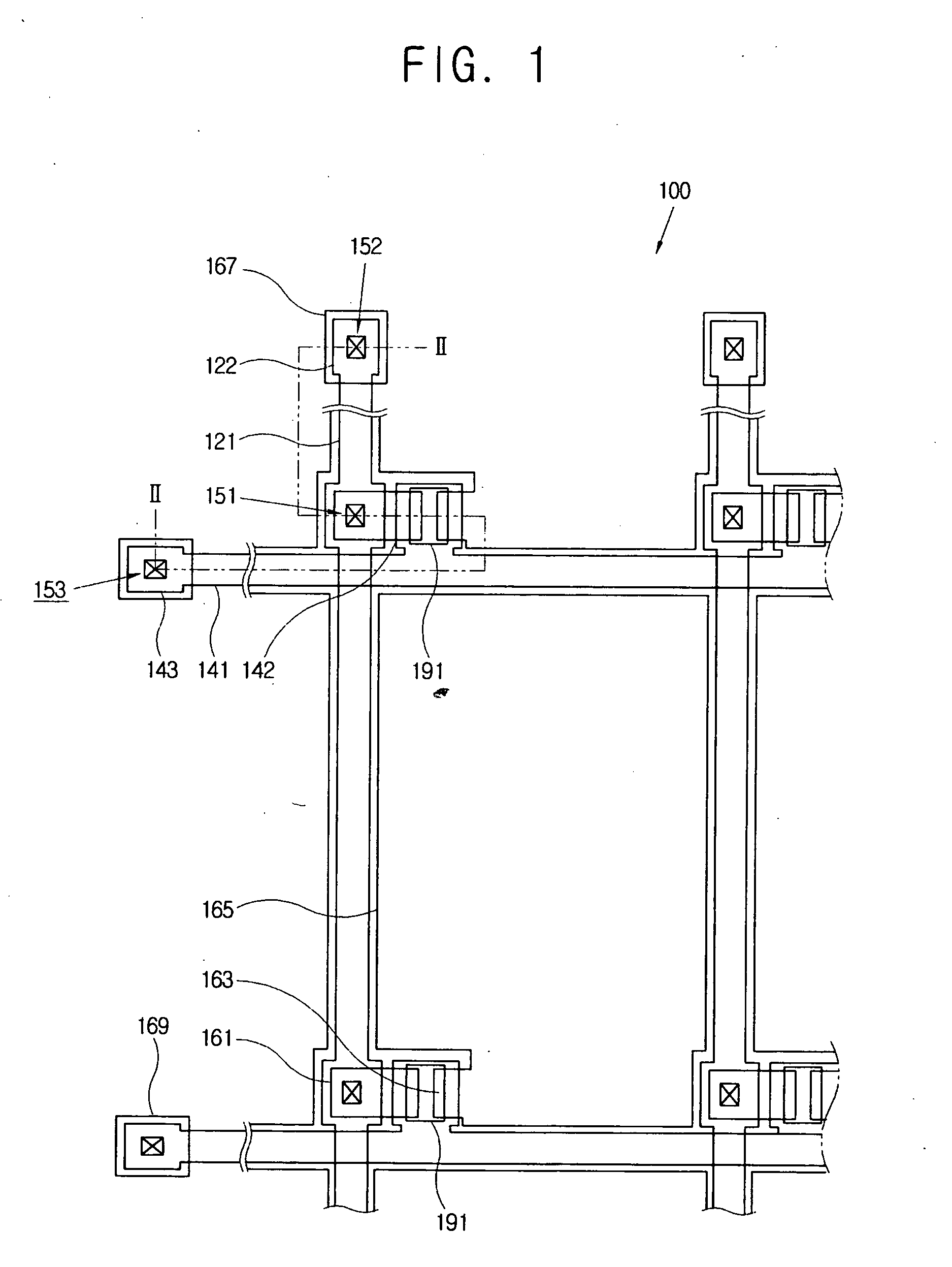
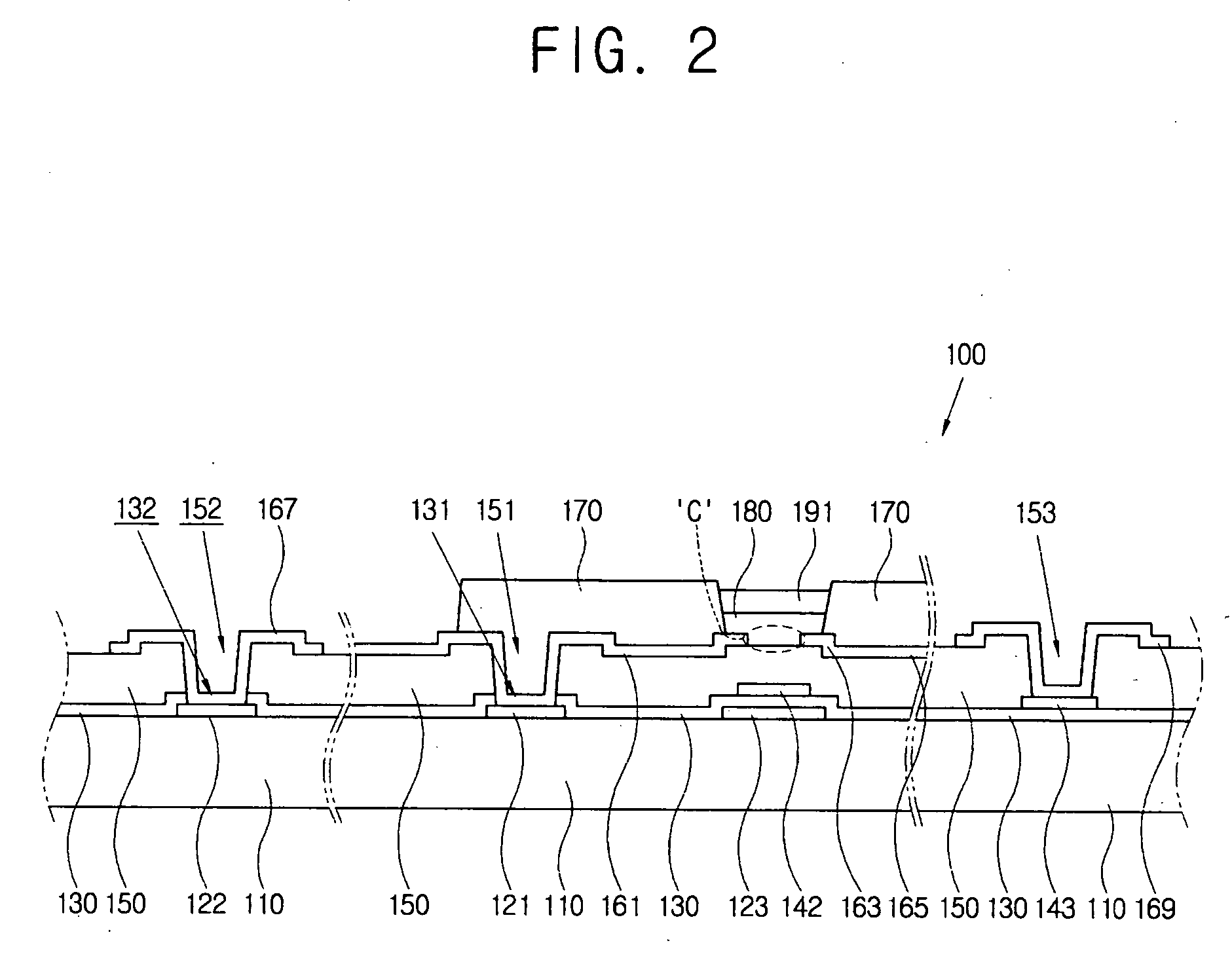
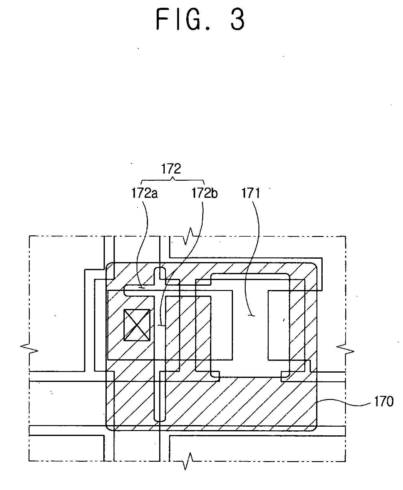
[0061] The ink guide part 172 according to the present invention comprises a first sub-guide part 172a extending outward from the channel part 171 and a second sub-guide part 172b crossing the first sub-guide part 172a. The first and the second sub-guide parts 172a and 172b overlap with at least one of the data wire (121, 122 and 123) and the gate wire (141, 142 and 143). Since the size of the wall 170 is increased, the processing margin of the ink-jet printing is improved. The size of wall 170 is increased, and the wall 170 overlaps with the data wire (121, 122 and 123) and the gate wire (141, 142 and 143). This configuration prevents reduction of aperture ratio due to the increased size of the wall 170. Further, increasing the size of the wall 170 and implementing the ink guide part 172 allows the organic semiconductor solution to be jetted more accurately on the openings 171 and 172. As a result, the organic semiconductor is more easily self-patterned, and the processing margin o...

third embodiment

[0066]FIG. 5 schematically illustrates a wall according to the present invention. As shown in FIG. 5, the wall 370 comprises an opening having a channel part 371 exposing a channel region, at least a portion of a source electrode and at least a portion of a drain electrode, and an ink guide part 372 extending outward from the channel part 371.

fourth embodiment

[0067]FIG. 6 schematically illustrates a wall according to the present invention. As shown in FIG. 6, the wall 470 comprises an opening with a channel part 471 positioned in one corner region of the wall 470 and an ink guide part 472 and 473 positioned in another corner region of the wall 470. The ink guide part 472 and 473 comprises a first sub-guide part 472 connected to the channel part 471 and a second sub-guide part 473 crossing the first sub-guide part 472.

[0068] The aforementioned first through fourth embodiments are not limited to the above descriptions, but may vary with different configurations. For example, more or fewer sub-guide parts may be used, and their general shape and positioning may be different than illustrated.

[0069] The wall according to the present invention may be employed in the fabrication of display devices such as liquid crystal displays (LCDs), organic light emitting diode (OLED) displays, and electro phoretic indication displays.

[0070] An OLED displ...


PUM


Abstract

Embodiments of a display device comprises an insulating substrate; a source electrode and a drain electrode on the insulating substrate and separated from one another to define a channel region; a wall having one or more openings to expose the channel region, at least a portion of the source electrode, and at least a portion of the drain electrode; and an organic semiconductor layer formed in the one or more openings, the one or more openings comprising a channel part exposing the channel region and an ink guide part extending outward from the channel part. The ink-jet printing process for the display device has an improved processing margin.

Description

CROSS-REFERENCE TO RELATED APPLICATIONS [0001] This application claims the benefit of Korean Patent Application No.2005-0112035, filed on Nov. 22, 2005, in the Korean Intellectual Property Office, the disclosure of which is incorporated herein by reference. BACKGROUND OF THE INVENTION [0002] 1. Field of the Invention [0003] The present invention relates to a display device and a manufacturing method thereof, and more particularly, to a display device and a manufacturing method thereof comprising an organic semiconductor layer. [0004] 2. Description of the Related Art [0005] A number of types of flat display devices are available; for example, liquid crystal displays (LCDs), organic light emitting diode (OLED) displays, etc. [0006] An LCD comprises an LCD panel having a thin film transistor (TFT) substrate where TFTs are provided, a color filter substrate where color filters are provided, and a liquid crystal layer disposed between the two substrates. [0007] The TFT substrate compris...

Claims


Application Information

Patent Timeline
Patent Type & Authority Applications(United States)
IPC IPC(8): H01L51/00H10K99/00
CPCH01L27/3244H01L51/0005H01L51/0012H01L51/0545H10K71/191H10K71/135H10K59/12H10K10/466H05B33/12
Inventor LEE, YONG-UKHONG, MUN-PYOKIM, BO-SUNGOH, JOON-HAKKIM, SOO-JIN
Owner SAMSUNG ELECTRONICS CO LTD
Why Eureka
Try Eureka