Light emitting element, production method thereof, backlight unit having the light emitting element, and production method thereof

a technology of light emitting elements and backlights, which is applied in the direction of optical elements, instruments, optics, etc., can solve the problems of reducing light emission efficiency or the element per se, unable to keep long-term reliability, and the light emitted from the led chip 103/b> cannot be efficiently guided to the light projecting surface of the light emitting element, etc., to achieve efficient heat dissipation, suppress light leakage, and enhance the intensity of light projected ou

Inactive Publication Date: 2007-05-24
BIOGENTIS +1
View PDF3 Cites 96 Cited by
  • Summary
  • Abstract
  • Description
  • Claims
  • Application Information

AI Technical Summary

Benefits of technology

[0021] The present invention was made in view of the foregoing problems, and an object of the present invention is to provide (i) a light emitting element in which long-term reliability is realized by enhancing intensity of light projected outward from a light projecting surface and by more efficiently radiating heat while suppressing light leakage, (ii) a production method thereof, and (iii) a backlight unit having the light emitting element.

Problems solved by technology

Further, if heat generated in the light emitting element is not sufficiently radiated, the heat damages members of the element, so that light emission efficiency drops or the element per se is damaged.
As a result, it is impossible to keep the long-term reliability.
Thus, the light emitted from the LED chip 103 cannot be efficiently guided to the light projecting surface of the light emitting element 101 and cannot be projected outward from the element.
Further, variation in an amount of the fluorescent particles changes scattering degree, so that the light cannot be stably projected outward.
However, in a conventional structure described in Tokukai 2005-223082, as a distance between an upper surface of the LED chip 103 and the reflecting film 121 is shorter, the light absorption / light leakage results in greater loss.
Hence, this raises such a problem that light is much less efficiently projected outward from the light emitting element.
This results in great energy loss in all.
Thus, light emitted from the LED chip cannot be efficiently projected outward, so that intensity of light projected from the light projecting surface decreases.

Method used


Image

  • Light emitting element, production method thereof, backlight unit having the light emitting element, and production method thereof
  • Light emitting element, production method thereof, backlight unit having the light emitting element, and production method thereof
  • Light emitting element, production method thereof, backlight unit having the light emitting element, and production method thereof

Examples


embodiment 1

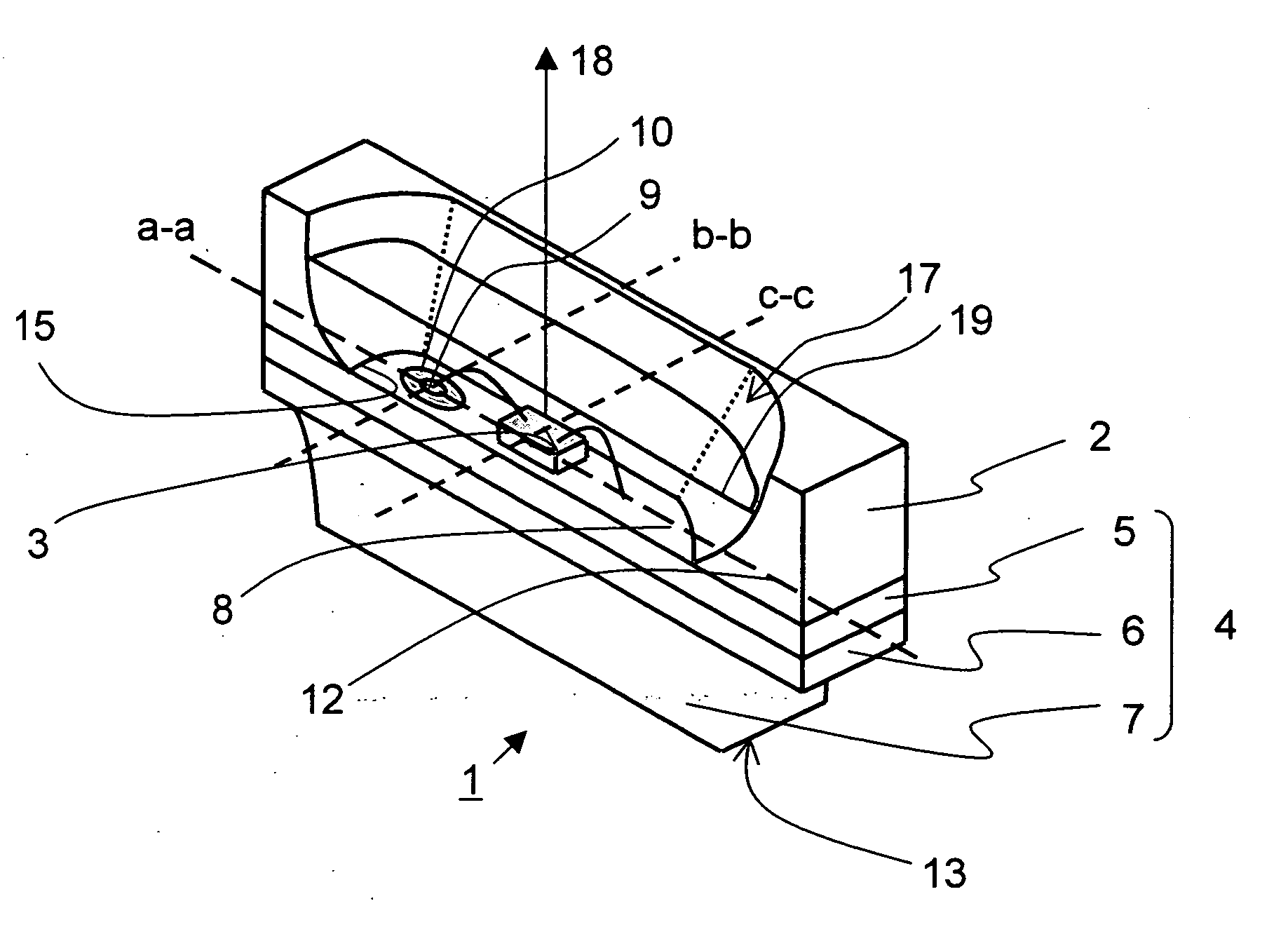
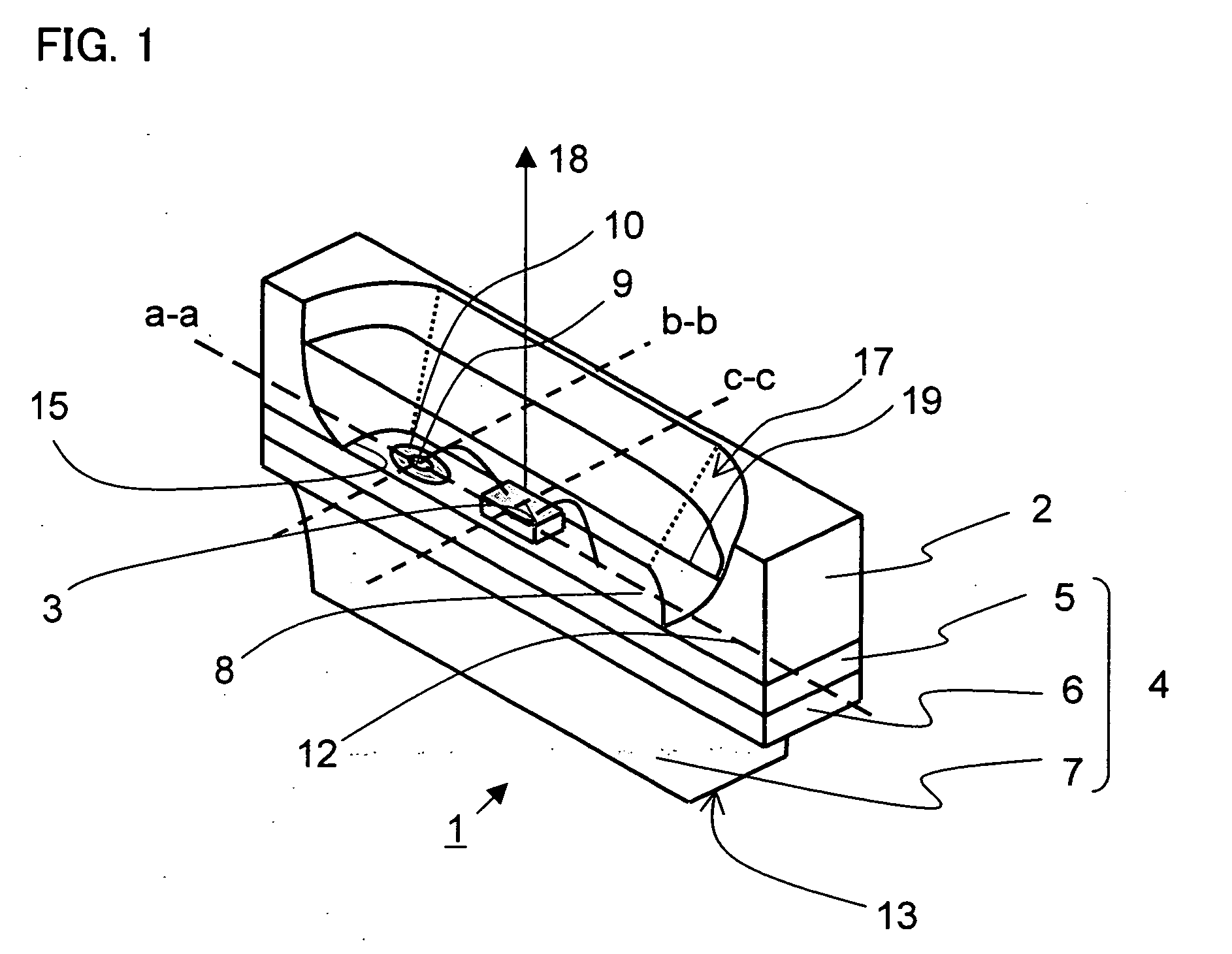
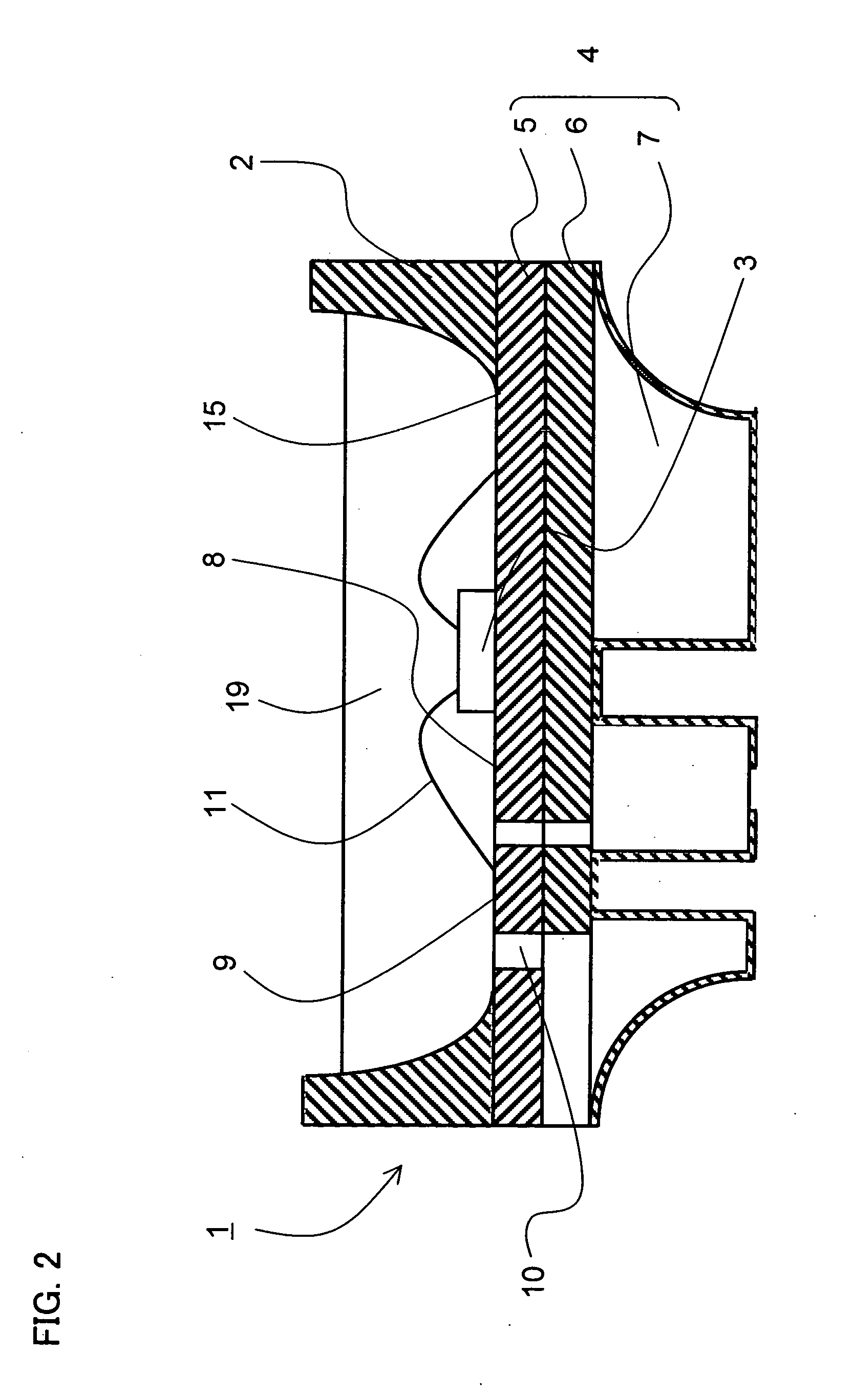
[0095] The following description will detail an embodiment of a light emitting diode chip according to the present invention with reference to attached drawings. FIG. 1 is an oblique perspective view of a light emitting element 1 in Embodiment 1 of the present invention, and FIG. 2 is a longer-side-direction cross sectional view of the light emitting element 1 (the view is taken along a line a-a), and FIG. 3 is a shorter-side-direction cross sectional view of the light emitting element 1 (the view is taken along a line b-b), and FIG. 4 is a shorter-side-direction cross sectional view of the light emitting element 1 (the view is taken along a line c-c).

[0096] As illustrated in FIGS. 1 to 4, an LED chip 3 is provided on a die-bond area / electrode section (first metallic portion) 8 positioned on a surface layer 5 (installation surface) of the laminate substrate 4. The LED chip 3 is a semiconductor chip, made of a GaN semiconductor material and the like, which includes electrode termina...

embodiment 2

[0112]FIG. 9 is an oblique perspective view of a liquid crystal panel backlight 20 of Embodiment 2. A light emitting element 1 illustrated in FIG. 9 is arranged in the same manner as the light emitting element 1 of Embodiment 1. As illustrated in FIG. 9, a side wall shield-free surface 12 of the light emitting element 1 is bonded to a reflective sheet 16 with a translucent adhesive. An optical waveguide 30 is provided in contact with the reflective sheet 16, and light emitted from the light emitting element 1 and being incident on the optical waveguide 30 is suitably scattered, which results in illumination from a backside of a liquid crystal panel 31. Note that, the reflective sheet 16 is generally used in combination with a laterally illuminating LED which laterally illuminates a thin display such as a liquid crystal panel, and the reflective sheet 16 serves as a part of the liquid crystal panel backlight unit as well as the optical waveguide 30. In the present invention, the refl...

embodiment 3

[0121] The following description will explain another embodiment of the present invention with reference to FIGS. 12 to 16.

[0122]FIG. 12 is an oblique perspective view illustrating an example of an arrangement of a light emitting element 500 of the present embodiment.

[0123]FIG. 13 is a cross sectional view which details the arrangement of the light emitting element 500.

[0124]FIG. 14 illustrates, as examples, etching patterns of a metallic reflecting plate 502 and respective layers of a laminate substrate 506. FIG. 14(a) illustrates a first layer 521, FIG. 14(b) illustrates a second layer 522, FIG. 14(c) illustrates a third layer 523, FIG. 14(d) illustrates a fourth layer 524, FIG. 14(e) illustrates a fifth layer 525, FIG. 14(f) illustrates a sixth layer 526, FIG. 14(g) illustrates a seventh layer 527, and FIG. 14(h) illustrates an eighth layer 528.

[0125] As illustrated in FIG. 12, the light emitting element 500 of the present embodiment includes: an LED chip 501 provided on a la...


PUM


Abstract

A light emitting element includes: A light emitting element, includes: at least one LED chip provided on an installation surface of a substrate; a metallic reflecting plate, provided upright in a light projecting direction of the LED chip on the installation surface so as to surround an entire periphery of the LED chip, the metallic reflecting plate reflecting light projected from the LED chip to guide the light to a light projecting surface provided in the light projecting direction; and a first metallic portion and a second metallic portion, respectively connected to the LED chip as electrode terminals for supplying a driving current to the LED chip, each being formed in an area surrounded by the metallic reflecting plate on the installation surface, wherein an insulating section is formed surrounding the second metallic portion, to electrically insulate the second metallic portion from other portion in the area, and the first metallic portion is formed outside the insulating section in the area as an installation surface metallic reflecting film so as to be in contact with the metallic reflecting plate.

Description

[0001] This Nonprovisional application claims priority under 35 U.S.C. § 119(a) on Patent Applications No. 337801 / 2005 filed in Japan on Nov. 22, 2005, No. 243327 / 2006 filed in Japan on Sep. 7, 2006, and No. 261567 / 2006 filed in Japan on Sep. 26, 2006, the entire contents of which are hereby incorporated by reference. FIELD OF THE INVENTION [0002] The present invention relates to (i) a light emitting element suitable for laterally illuminating a thin display such as a liquid crystal panel, (ii) a production method thereof, (iii) a backlight unit having the light emitting element and (iv) a production method thereof. BACKGROUND OF THE INVENTION [0003] Conventionally, as a backlight for laterally illuminating a display panel of liquid crystal or the like, a light emitting element such as a laterally light emitting diode (hereinafter, referred to as “LED”) disclosed in, for example, Japanese Unexamined Patent Publication No. 223082 / 2005 ((Tokukai 2005-223082)(Publication date: Aug. 18,...

Claims


Application Information

Patent Timeline
Patent Type & Authority Applications(United States)
IPC IPC(8): H01L33/00H01L33/32H01L33/46H01L33/56H01L33/60H01L33/62H01L33/64
CPCG02B6/0031G02B6/0073G02B6/0083H01L25/0753H01L33/483H01L33/60H01L33/62H01L33/64H01L33/647H01L2224/48227H01L2224/48091H01L2924/00014H01L2924/3025H01L2924/00H01L2924/181H01L2924/18301H01L2924/00012
Inventor TAKEMOTO, MASASHITAKIGUCHI, HARUHISAOGATA, NOBUOUKAI, KENICHI
Owner BIOGENTIS
Why Eureka
Try Eureka