Methods and systems for high write performance in multi-bit flash memory devices

a multi-bit flash memory and write speed technology, applied in the field of memory devices, can solve the problems of limiting the use of flash memory devices in applications requiring high-speed programming, the speed at which flash memory is programmed is somewhat limited, etc., and achieves the effect of positive impact on write speed, fast programming, and fast programming

Active Publication Date: 2007-05-24
III HLDG 4
View PDF13 Cites 5 Cited by
  • Summary
  • Abstract
  • Description
  • Claims
  • Application Information

AI Technical Summary

Benefits of technology

[0015] In accordance with one aspect of the invention, a method of programming one or more dual-bit flash memory cells is provided. The method comprises erasing first and second bits of each cell within a portion of the array to a first or an initial state, and then programming the first bit of each dual-bit cell in the array portion to a second state. The method further comprises subsequently programming the second bit of one or more of the cells in the array portion to one of the first and second state based on data input by a user. In the above method, the first bit of each dual-bit cell is not employed for user's data retention, but instead is used to positively impact the write speed (make faster) of the corresponding second bit associated therewith during subsequent programming operations. In the above instance, either of the first or second bit locations can be interchanged as the “don't care” bit location, with fast programming effectuated with the other bit location within the cell. Although reducing user's data retention density, the above method has been found to provide improved programming speeds by about 4 times or more over conventional programming of the 2 bits in dual-bit flash, or the single bit of NAND flash.
[0016] In accordance with another aspect of the present invention, a method of erasing dual-bit flash memory cells comprises removing charge from first and second bit locations of each cell within a predetermined portion of a flash memory array. In one example, the amount of charge removed from the first and second bit locations is sufficient to force each of the bits to a first state. The method further comprises applying charge to the first bit location of each of the dual-bit cells within the predetermined portion of the array. Subsequently, a programming operation is performed, wherein the second bit locations of one or more dual-bits cells within the predetermined portion of the array are programmed to one of the two possible states, based on data input by a user. Again, swapping the first and second bit locations as the “don't care” bit location for each cell in the array portion is contemplated by the present invention. The application of charge to the first bit locations, in the present example, increases substantially the speed at which user's data may be subsequently written to the second bit locations associated with such cells. In one example, any amount of charge is supplied to the first bit locations, while in another example the charge supplied thereto is sufficient to change the first un-programmed bit locations to a second (programmed) state. In one example, applying charge to one of the bits in the cells is done during the embedded erase (or pre-condition) process, to enable a fast write of user's data in the other bit of the cells later on.
[0020] The present invention is also directed to a dual-bit memory comprising a core cell array of dual-bit flash memory cells configured into a plurality of array portions (e.g., sectors). The memory further comprises a control circuit configured to partition the plurality of array portions into one of a fast write array portion and a normal write array portion (wherein both portions are not necessarily continuous). In addition, in one example, the control circuit further comprises fast write control logic configured to perform a fast write block erase operation on designated fast write array portions partitioned in the array. The fast write control logic is, for example, configured to block erase both first and second bit locations of each dual-bit cell in the fast array portion by removing charge therefrom. The control logic is further configured to supply charge to the first bit location of each cell in the fast array portion to thereby facilitate fast write operations subsequently to the second bit locations of any cell within the fast write array portion.
[0021] In another aspect of the present invention, a dual-bit flash memory comprises a core cell array of dual-bit flash memory cells configured into a plurality of array portions such as memory sectors. The memory further comprises a control circuit adapted to selectively block erase one of the array portions designated for fast write operations in two phases, wherein a first phase comprises block erasing both first and second bit locations of each cell therein to a first state. The control circuit is further adapted, in a second phase, to supply charge to the first bit location of each of the block erased cells. In one example, the charge supplied thereto is sufficient to render the first bit location to be read as a second state. Subsequently, the fast write array portion may have user's data programmed to the second bit locations of one or more cells therein at a rate substantially faster than conventional memory architectures.

Problems solved by technology

For example, presently the speed at which flash memory is programmed is somewhat limited, thereby limiting the use of flash memory devices in applications requiring high-speed programming.

Method used


Image

  • Methods and systems for high write performance in multi-bit flash memory devices
  • Methods and systems for high write performance in multi-bit flash memory devices
  • Methods and systems for high write performance in multi-bit flash memory devices

Examples


Embodiment Construction

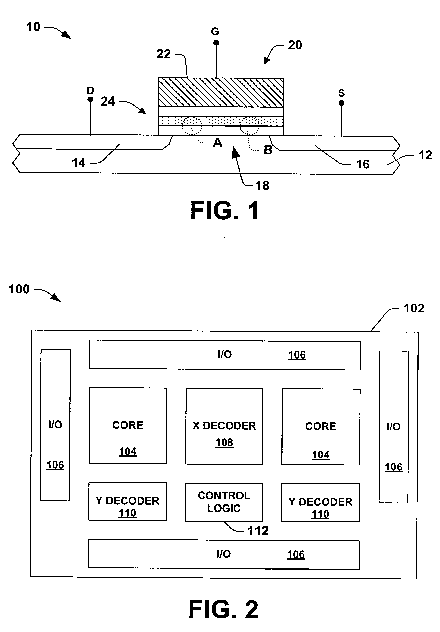
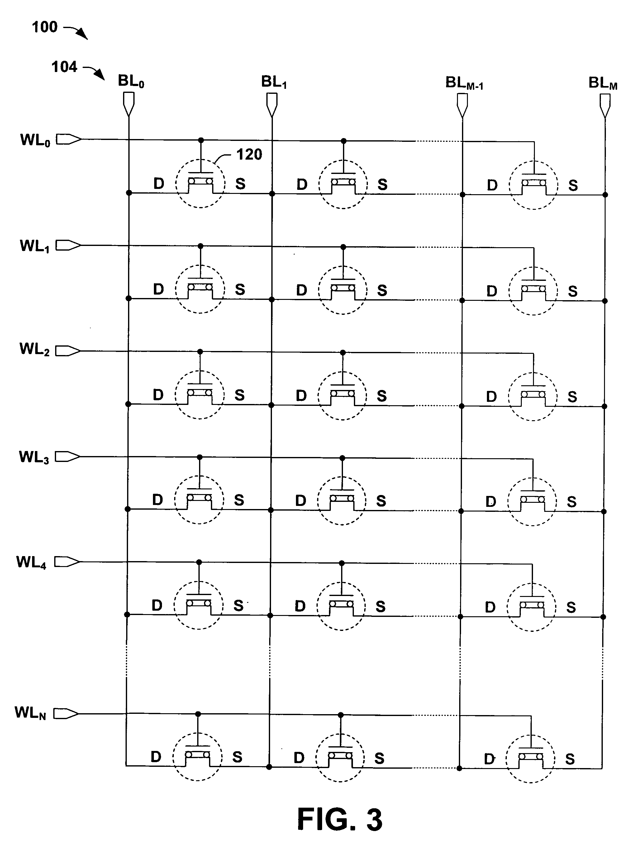
[0036] One or more implementations of the present invention will now be described with reference to the drawings, wherein like reference numerals are used to refer to like elements throughout. One or more aspects of the invention are hereinafter illustrated and described in the context of an exemplary dual-bit flash memory device in which conductive doped polysilicon word lines are formed above a charge trapping layer to create flash memory cells in combination with diffused bit line portions (e.g., source / drains) in an underlying silicon semiconductor body, with the cells organized along rows (e.g., word lines) and columns (e.g., bit lines) in a virtual ground array. However, the invention is not limited to the illustrated implementations and may alternatively be employed in connection with any specific type of substrate materials (e.g., silicon wafer, SOI wafer, epitaxial layer, etc.), any type of dual-bit flash memory cell structure, and any array configuration (e.g., NOR, virtua...


PUM


Abstract

Methods and circuits are presented for performing high speed write (programming) operations in a dual-bit flash memory array. The method includes, for example, erasing a first and second bit of each cell in the array to a first state, programming the first bit of each cell in the array to a second state, and subsequently programming the second bit of one or more cells in the array to one of the first and second state according to the user's data, resulting in fast write (programming) of those second bits. In addition, the circuit includes, for example, a core cell array having dual-bit flash memory cells configured into a plurality of array portions. The circuit further includes a control circuit configured to selectively block erase one of the array portions, wherein in a first phase of the block erase both first and second bit locations of each dual-bit flash memory cell in the one array portion have sufficient charge removed therefrom to achieve a first state. The control circuit is further configured to, in a second phase of the block erase, supply charge to the first bit location of each dual-bit flash memory cell of the one array portion to enable subsequently fast-write of user's data to the second bit location.

Description

REFERENCE TO RELATED APPLICATION [0001] This application is a divisional application of U.S. patent application Ser. No. 11 / 037,477 which was filed Jan. 18, 2005, entitled METHODS AND SYSTEMS FOR HIGH WRITE PERFORMANCE IN MULTI-BIT FLASH MEMORY DEVICES that claims the benefit of U.S. Provisional Patent Application Ser. No. 60 / 563,046 which was filed Apr. 16, 2004, entitled METHODS AND SYSTEMS FOR HIGH WRITE PERFORMANCE IN MULTI-BIT FLASH MEMORY DEVICES.FIELD OF INVENTION [0002] The invention is generally related to the field of memory devices and more particularly to methods and systems for high speed programming in multi-bit flash memory devices. BACKGROUND OF THE INVENTION [0003] Flash and other types of electronic memory devices are constructed of memory cells that individually store and provide access to data. A first generation type memory cell stores a single binary piece of information referred to as a bit, which has one of two possible states. The cells are commonly organize...

Claims


Application Information

Patent Timeline
Patent Type & Authority Applications(United States)
IPC IPC(8): G11C16/04G11C11/56G11C16/10
CPCG11C16/0475G11C16/10G11C2211/5641G11C11/56G11C16/04G11C16/14G11C16/16
Inventor RANDOLPH, MARKHAMILTON, DARLENEKORNITZ, RONI
Owner III HLDG 4
Why Eureka
Try Eureka