
Semiconductor device and method of fabricating the same

Active Publication Date: 2007-05-31
SAMSUNG ELECTRONICS CO LTD
View PDF3 Cites 8 Cited by
  • Summary
  • Abstract
  • Description
  • Claims
  • Application Information

AI Technical Summary

Benefits of technology

[0009] Accordingly, the present invention has been made keeping in mind the above problems occurring in the related art, and a feature of the present invention is to provide a semiconductor device having improved resistance properties and high reliability.

Problems solved by technology

As well, copper has low resistivity.
However, copper suffers because it diffuses in an insulating film formed of silicon or silicon oxide used in the semiconductor device, undesirably increasing current leakage or parasitic capacitance.
However, the diffusion barrier, having higher resistance than copper, is disadvantageously provided at the bottom of the via hole connecting the upper wire and the lower wire, leading to increased wire resistance.
Such SIV results in poor electrical properties of the wire, deteriorating the reliability of the semiconductor device.

Method used


Image

  • Semiconductor device and method of fabricating the same
  • Semiconductor device and method of fabricating the same
  • Semiconductor device and method of fabricating the same

Examples


Embodiment Construction

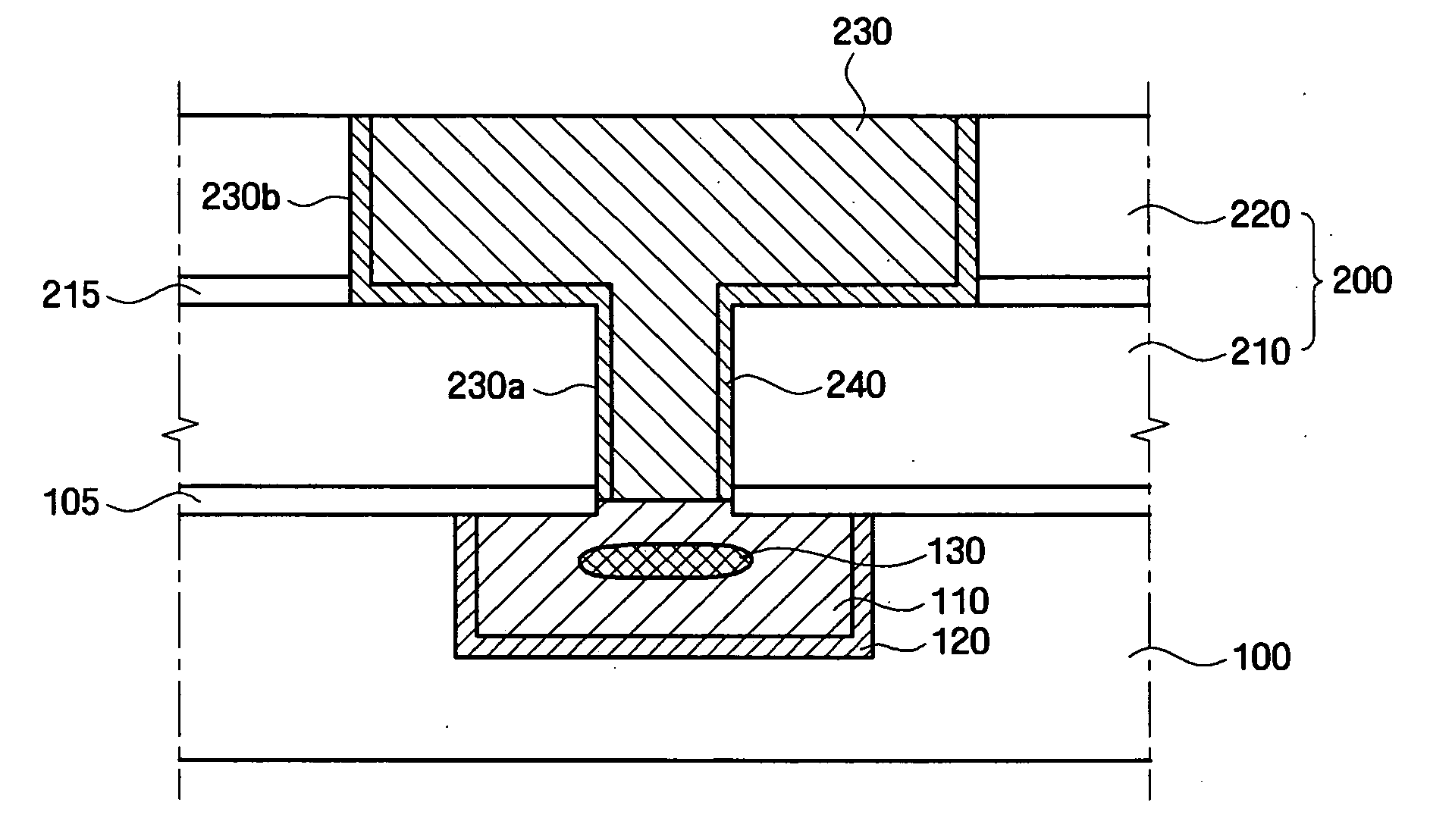
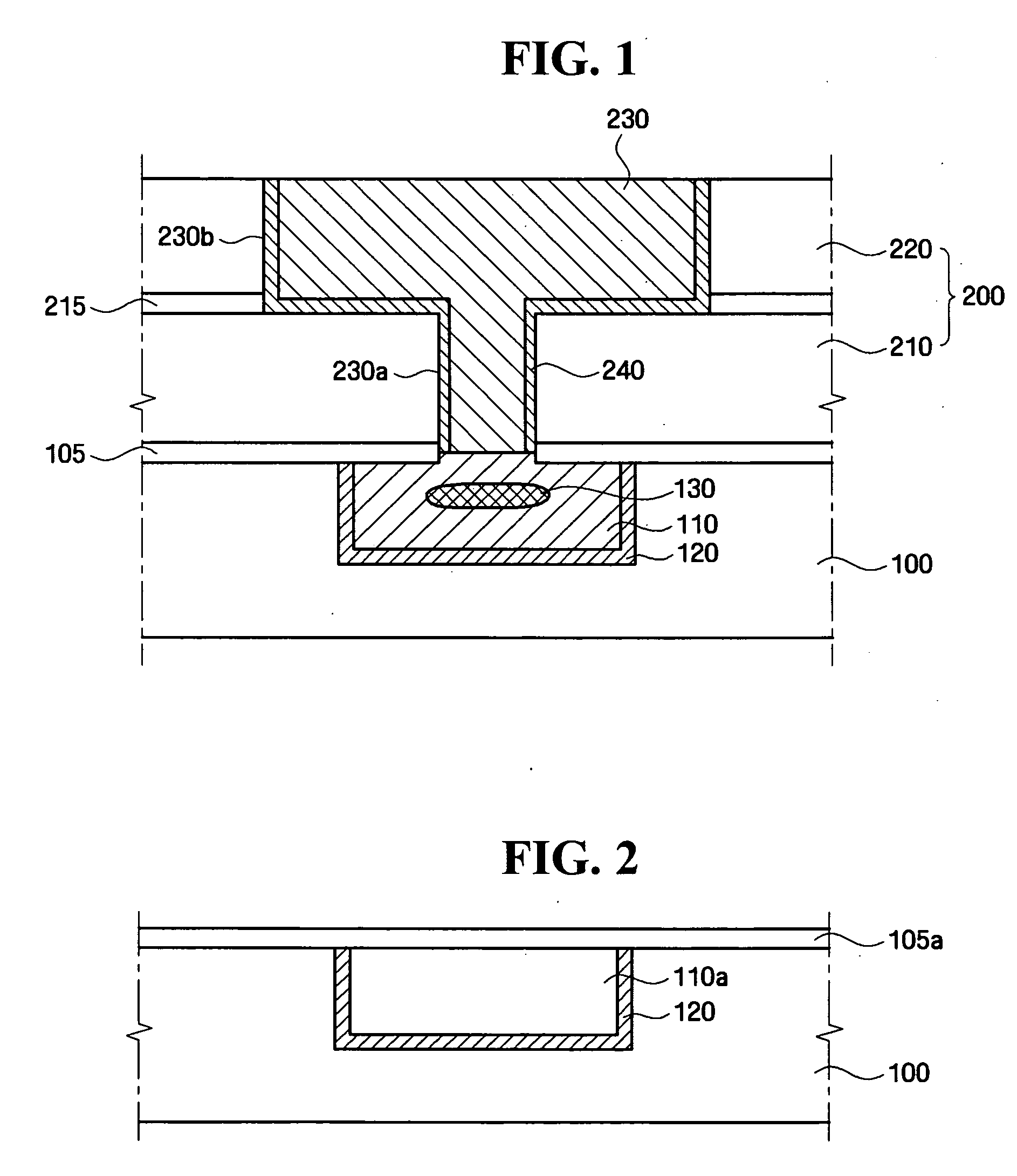
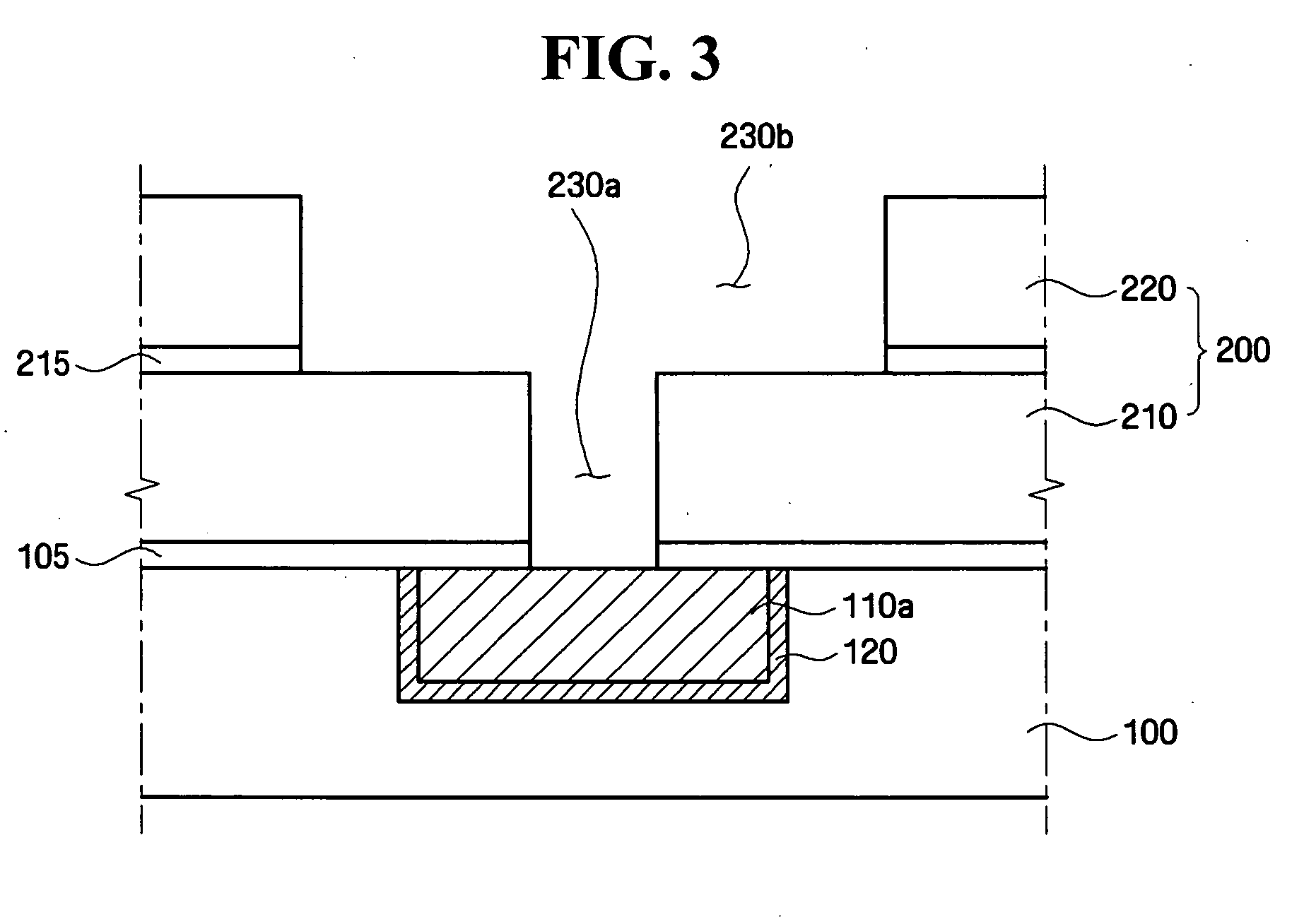
[0029] The advantages and features of the present invention, and the way of attaining them, will become apparent with reference to embodiments described below in conjunction with the accompanying drawings. However, the present invention is not limited to the embodiments disclosed below and will be embodied in a variety of different forms; rather, these embodiments are provided so that this disclosure will be thorough and complete, and will fully convey the scope of the present invention to those skilled in the art, and the scope of the present invention will be defined by the appended claims.

[0030] Reference now should be made to the drawings, in which the same reference numerals are used throughout the different drawings to designate the same or similar components. Further, the embodiments of the present invention are described, with reference to cross-sectional views provided as ideal illustrations of the present invention. As such, the type of illustration may vary depending on ...


PUM


Abstract

A semiconductor device and a method of fabricating the same are disclosed. The semiconductor device includes a lower wire, an interlayer insulating film formed on the lower wire and having a via hole exposing the upper surface of the lower wire, a diffusion barrier formed on the inner wall of the via hole, and an upper wire filling the via hole and directly contacting the lower wire, in which a dopant region containing a component of the diffusion barrier is formed in the lower wire in the extension direction of the via hole.

Description

CROSS-REFERENCE TO RELATED APPLICATION [0001] This application is based on and claims priority from Korean Patent Application No. 10-2005-0113818 filed on Nov. 25, 2005 in the Korean Intellectual Property Office, the disclosure of which is incorporated herein in its entirety by reference. BACKGROUND OF THE INVENTION [0002] 1. Field of the Invention [0003] The present invention relates to a semiconductor device and a method of fabricating the same and, more particularly, to a semiconductor device having highly reliable wires and a method of fabricating such a semiconductor device. [0004] 2. Description of the Related Art [0005] With the increase in the degree of integration of a semiconductor device, the requirement for reliable wires is increasing. As wiring material of the semiconductor device, copper (Cu) has a higher melting point than aluminum (Al), and thus exhibits excellent electro-migration (EM) and stress-migration (SM) properties. As well, copper has low resistivity. [0006...

Claims


Application Information

Patent Timeline
IPC IPC(8): H01L23/02
CPCH01L21/76844H01L21/76864H01L21/76886H01L23/53238H01L2924/0002H01L2924/00H01L21/28
Inventor OH, JUN-HWANMAENG, DONG-CHOKIM, SOON-HO
Owner SAMSUNG ELECTRONICS CO LTD
Features
  • Generate Ideas
  • Intellectual Property
  • Life Sciences
  • Materials
  • Tech Scout
  • Unparalleled Data Quality
  • Higher Quality Content
  • 60% Fewer Hallucinations
Learn More