Substrate cleaning method, substrate cleaning apparatus and computer readable recording medium

Inactive Publication Date: 2007-06-14
TOKYO ELECTRON LTD
View PDF4 Cites 48 Cited by
  • Summary
  • Abstract
  • Description
  • Claims
  • Application Information

AI Technical Summary

Benefits of technology

[0025] According to the invention, even when a mixture a hydrophobic surface and a hydrophilic surface exists, it is possible to make the difference between the dry time for the hydrophobic surface and the dry time for the hydrophilic surface smaller, so that a h

Problems solved by technology

Such a process method has a problem such that water marks is generated on the surface of a semiconductor wafer by adhesion of a mist of pure water, which is generated at the time of spin dry, to the dry surface of the semiconductor wafer, or the like.

Method used


Image

  • Substrate cleaning method, substrate cleaning apparatus and computer readable recording medium
  • Substrate cleaning method, substrate cleaning apparatus and computer readable recording medium
  • Substrate cleaning method, substrate cleaning apparatus and computer readable recording medium

Examples


Embodiment Construction

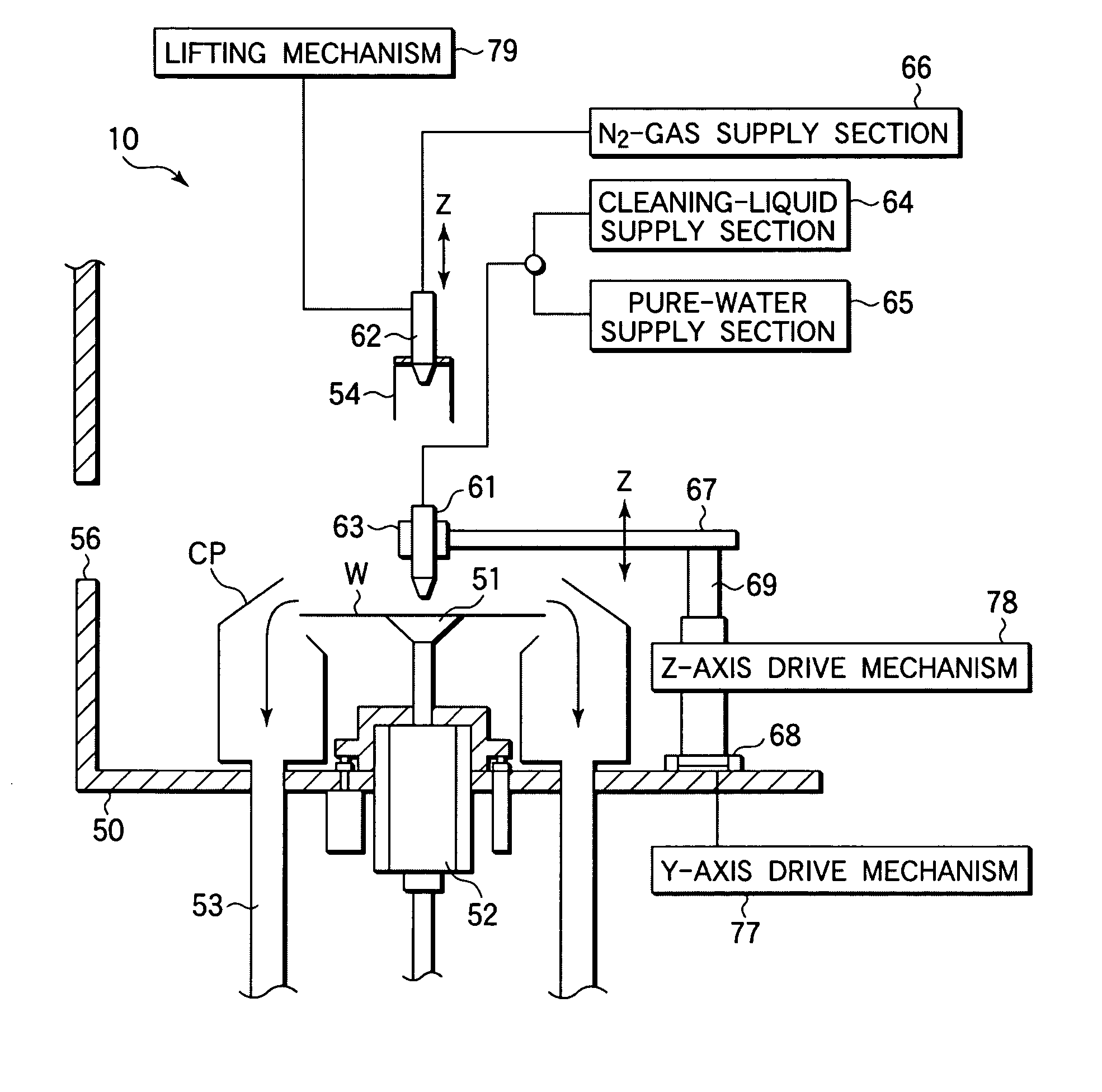
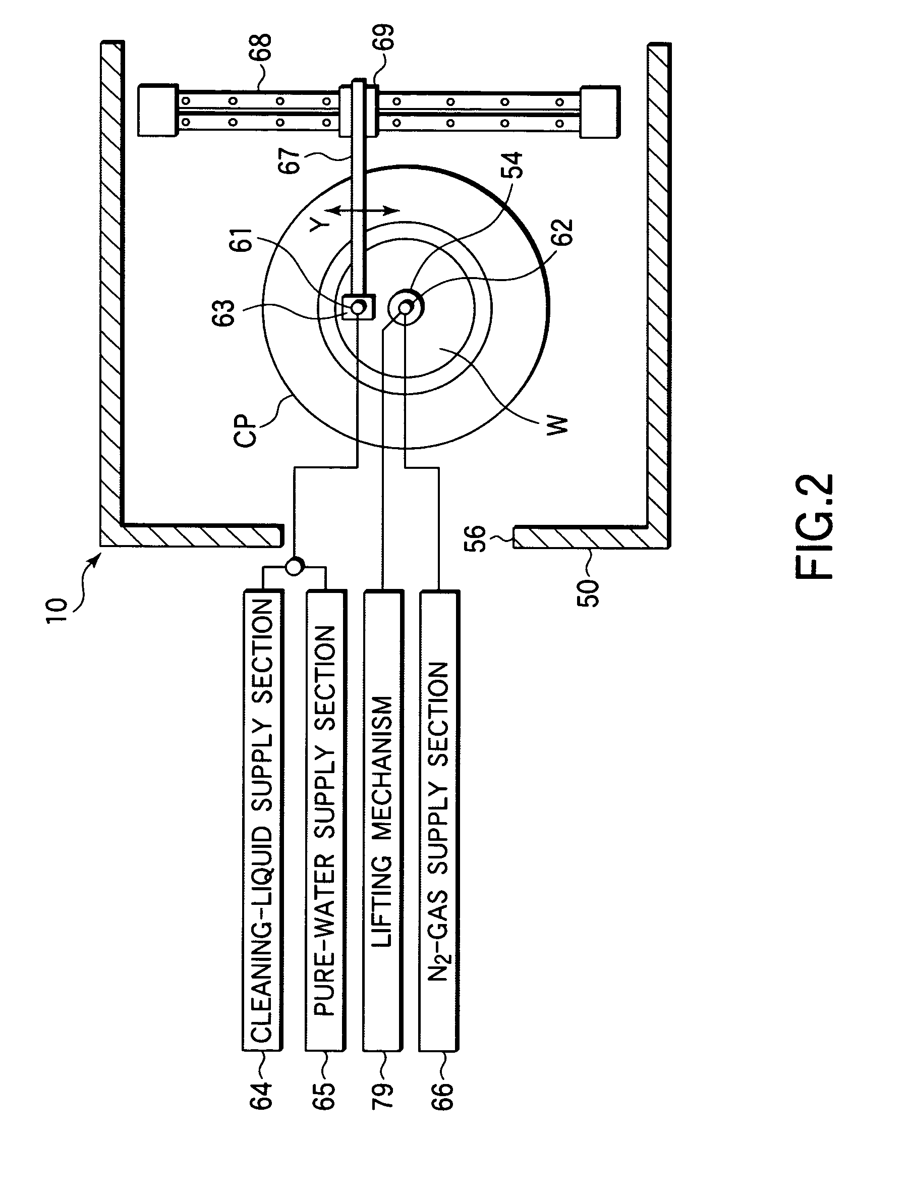
[0037] An embodiment of the present invention will be described below with reference to the accompanying drawings. FIG. 1 presents a vertical cross-sectional view showing the schematic structure of a substrate cleaning apparatus 10 which cleans a semiconductor wafer, and FIG. 2 presents a plan view thereof.

[0038] The essential portions of the substrate cleaning apparatus 10 are provided in a casing 50. FIG. 1 and FIG. 2 show only a part of the casing 50. A ring-shaped cup CP is disposed in approximately the center of the casing 50, and a spin chuck 51 is placed inside the cup CP. A chuck which vacuum-chucks and holds a wafer W, or a so-called mechanical chuck type, such as one which mechanically holds the end faces of the wafer W, is preferably used as the spin chuck 51, which is rotated while holding the wafer W by a drive motor 52. A drain 53 for discharging a cleaning liquid and pure water is provided in the bottom of the cup CP, and a feed window 56 through which a wafer is tra...


PUM


Abstract

After a rinse process on a wafer W is performed by feeding pure water to the surface of the wafer W at a predetermined flow rate while rotating the wafer W in an approximately horizontal state, a feed amount of the pure water to the wafer W is reduced, and a pure-water feed point is moved outward from the center of the wafer W. In this manner, the wafer W is subjected to a spin dry process while forming a liquid film in a substantially outer region of the pure-water feed point.

Description

TECHNICAL FIELD [0001] The present invention relates to a substrate cleaning method capable of suppressing generation of water marks on the surface of a substrate to be processed, such as a semiconductor wafer or a glass substrate for FPD (Flat Panel Display), a substrate cleaning apparatus and a computer readable recording medium for executing the substrate cleaning method. BACKGROUND ART [0002] In a semiconductor device fabrication process, for example, as the surface of a semiconductor wafer should always be kept clean, a cleaning process is performed on the semiconductor wafer approximately. As a typical example of a single wafer type cleaning process of processing semiconductor wafers one by one, a process method is known which feeds a predetermined cleaning liquid to a semiconductor wafer held by a spin chuck (chemical liquid cleaning process), then feeds pure water to the semiconductor wafer to rinse the cleaning liquid (rinse process), and further rotates the semiconductor w...

Claims


Application Information

Patent Timeline
IPC IPC(8): B08B7/00B08B3/00B08B3/02G11B23/50H01L21/00H01L21/304H01L21/306
CPCB08B3/02G02F2001/1316H01L21/67051H01L21/67034G11B23/505G02F1/1316H01L21/304
Inventor NANBA, HIROMITSUYABUTA, TAKASHIORII, TAKEHIKO
Owner TOKYO ELECTRON LTD
Why Eureka
Try Eureka