Supercharge Your Innovation With Domain-Expert AI Agents!

Method and structure of an one time programmable memory device in an embedded EEPROM

a one-time programmable and memory integrated device technology, applied in the field of integrated circuits, can solve the problems of small devices, and difficult to integrate devices on a single chip, and achieve the effect of reducing the long lead time in coding

Active Publication Date: 2007-06-14
SEMICON MFG INT (SHANGHAI) CORP
View PDF2 Cites 4 Cited by
  • Summary
  • Abstract
  • Description
  • Claims
  • Application Information

AI Technical Summary

Benefits of technology

[0012] Many benefits are achieved by way of the present invention over conventional EEPROM and masked ROM. For example, the resulting OTP EPROM has a reduced cell size that is about 0.8-1.2 μm2 and less and the EEPROM has a cell size of about 3-6 μm2 and less, using a 0.18 μm technology node. The present invention also provides the benefit of an embedded OTP device that eliminates the long lead time in coding as required in a masked ROM. Additionally, the method provides a process that is compatible with conventional process technology without substantial modification to convention equipment and process. Depending upon the embodiment, one or more of the these benefits may be achieved. These and other benefits will be described in more throughout the present specification and more particularly below.

Problems solved by technology

An integrated circuit or chip fabrication facility can cost hundreds of millions, or even billions, of dollars.
Making devices smaller and integrating device function on a single chip is very challenging, as each process used in integrated device fabrication has a limit.
Although such mask ROMs have been successful, conventional mask ROMs have certain limitations.
That is, such conventional mask ROMs often suffer from a long coding lead time and inflexibility.
The result is higher manufacturing cost.

Method used


Image

  • Method and structure of an one time programmable memory device in an embedded EEPROM
  • Method and structure of an one time programmable memory device in an embedded EEPROM
  • Method and structure of an one time programmable memory device in an embedded EEPROM

Examples


Embodiment Construction

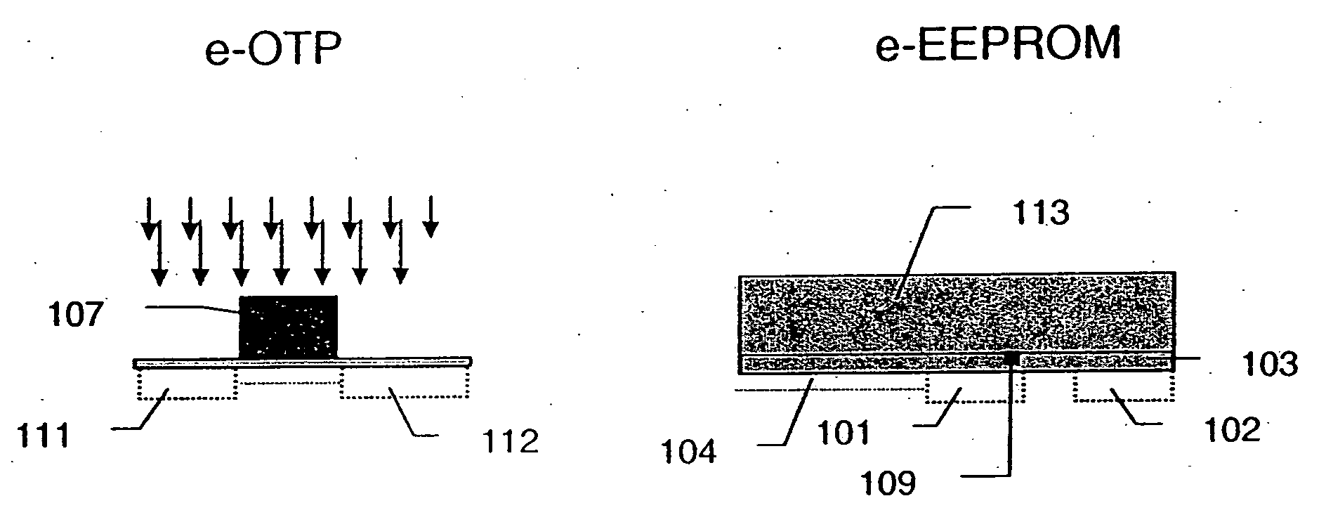
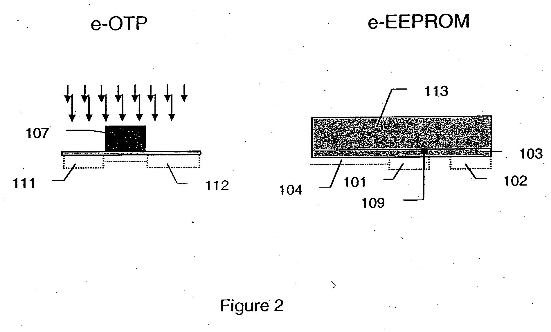
[0021] The present invention provides a fabrication method for a one time programmable (OTP) memory device in an embedded EEPROM array. In particular, the invention provides a method and resulting device for manufacturing a OTP EPROM device structure in an embedded EEPROM array. But it would be recognized that the invention has a much broader range of applicability.

[0022] A method for fabricating a OTP EPROM device in an embedded EEPROM array according to the present invention may be outlined as follows:

[0023] 1. Provide a semiconductor substrate including a surface region;

[0024] 2. Provide a first cell region and a second cell region;

[0025] 3. Form a gate dielectric layer of a first thickness overlying the surface region of the substrate;

[0026] 4. Form a tunnel oxide window of a second thickness in a portion of the second cell region;

[0027] 5. Form a first OTP EPROM gate associated with an OTP EPROM gate structure overlying the gate dielectric layer in the first cell region, ...


PUM


Abstract

A structure and a manufacturing method for an OTP-EPROM in an embedded EEPROM integrated circuit structure. The structure has a substrate that includes a surface region. The structure has a gate dielectric is overlying the surface region. The structure also a first OTP-EPROM gate overlying the gate dielectric layer in a first cell region, and an EEPROM floating gate and a select gate overlying the gate dielectric layer in a second cell region. An insulating layer is overlying the first OTP-EPROM gate, the EEPROM floating gate and the select gate. An OTP-EPROM control gate is overlying the insulating layer and coupled to the first OTP-EPROM gate. An EEPROM control gate is overlying the insulating layer and coupled to the EEPROM floating gate.

Description

BACKGROUND OF THE INVENTION [0001] The present invention relates to an integrated circuit that employs a combination of multiple non volatile memory cell structures. More particularly the present invention relates to a highly integrated circuit and a fabrication method for an one time programmable (OTP) memory integrated device in an embedded EEPROM array. Merely by way of example, the invention has been applied to an one time programmable erasable programmable read only memory (OTP EPROM) device in an embedded EEPROM array. But it would be recognize that the invention has a much broader applicability. [0002] Integrated circuits have evolved from a handful of interconnected devices fabricated on a single chip of silicon to millions of devices. Conventional integrated circuits provide performance and complexity far beyond what was originally imagined. In order to achieve improvements in complexity and circuit density (i.e., the number of devices capable of being packed onto a given c...

Claims


Application Information

Patent Timeline
IPC IPC(8): H01L29/788
CPCH01L27/115H01L27/11519H01L27/11521H01L27/11524H10B41/10H10B41/35H10B69/00H10B41/30
Inventor CHAN, YIPENGHUANG, SHENGHELU, JING
Owner SEMICON MFG INT (SHANGHAI) CORP
Features
  • R&D
  • Intellectual Property
  • Life Sciences
  • Materials
  • Tech Scout
  • Unparalleled Data Quality
  • Higher Quality Content
  • 60% Fewer Hallucinations
Learn More