Suppression method and structure for reducing a via stub effect of a substrate

a technology of substrate and via stub, which is applied in the direction of printed circuit aspects, multiple-port networks, high frequency circuit adaptations, etc., can solve the problems of skin effect, dielectric loss, and affect the characteristics of signals transmitted in such an environment, so as to save the extra drilling time and cost, and reduce the via stub effect of the substrate

Inactive Publication Date: 2007-06-14
INVENTEC CORP
View PDF4 Cites 13 Cited by
  • Summary
  • Abstract
  • Description
  • Claims
  • Application Information

AI Technical Summary

Benefits of technology

[0008] Another objective of the present invention is to provide a suppression method and structure for reducing the via stub effect of the substrate, to save the extra drilling time and cost.
[0009] A further objective of the present invention is to provide a suppression method and structure for reducing the via stub effect of the substrate, to avoid the negative effects such as parasite capacitance on the via open stub under circumstance that not affecting the wiring space on the substrate.
[0010] In accordance with the above and other objectives, the present invention provides a suppression method for reducing the via stub effect of the substrate, applying on the substrate which has via and uses electrical connection to connect the first conductive line and the second conductive line. The suppressing method includes changing a first width of a first conductive segment of the first conductive line connected to the via, and changing a second width of a second conductive segment of the second conductive line connected to the via, so as to change impedances of the first conductive line and the second conductive line to match with a stub impedance of the via, reduce a parasite impedance of the via stub, reach an impedance match at a designed frequency point, and improve an integrity of a signal after traveling from the first conductive line, the via and the second conductive line.
[0011] The suppression method for reducing the via stub effect of the substrate of the present invention adopts a Smith Chart to adjust

Problems solved by technology

With the demands asked by circuits operating at a high speed for bandwidth keep growing, loss, reflection and crosstalk effects are becoming three of the most important issues in the art.
The problem regarding to the signal integrity occurs if a transmission rate is as high as several Gbps, causing some serious problems such as skin effect, dielectric loss, reflection, crosstalk, and inter-symbol interference (ISI).
The substrate is a complex environment comprising by many different elements, and now it has become a challenge for the signal transmission rate up to several Gbps.
In result, characteristics of signals transmitted in such an environment are affected.
However, when the circuit is operating at a high speed, with the differences in signal layer (and the via through/stub

Method used


Image

  • Suppression method and structure for reducing a via stub effect of a substrate
  • Suppression method and structure for reducing a via stub effect of a substrate
  • Suppression method and structure for reducing a via stub effect of a substrate

Examples


Embodiment Construction

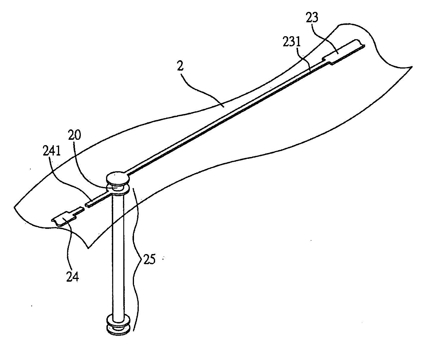
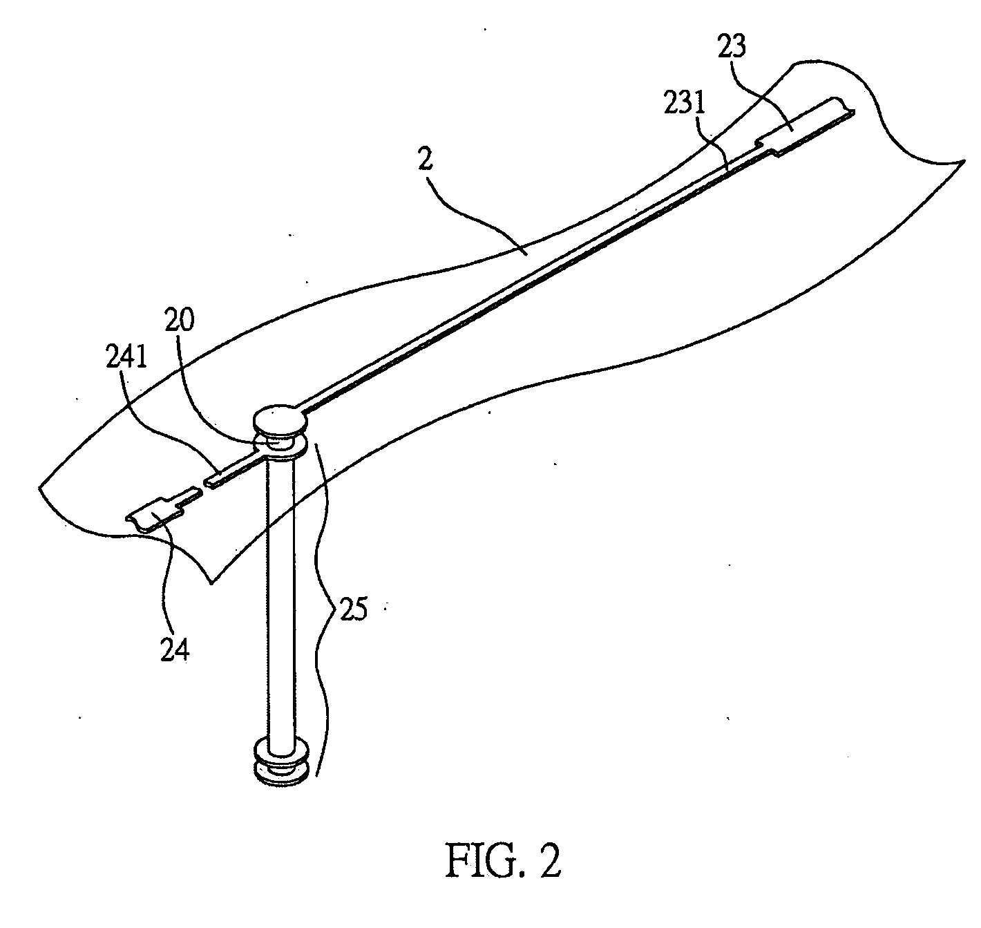
[0018]FIG. 2 illustrates an exemplary preferred embodiment of the present invention, which provides a suppression method for reducing the via stub effect of the substrate, applying on the substrate 2 which has via 20 and uses electrical connection to connect the first conductive line 23 and the second conductive line 24. The suppression method is to change widths of two conductive segments 231 and 241 of the first conductive line 23 and the second conductive line 24 connecting to the via 20, in order to change impedances of the conductive segments 231 and 241 of the first conductive line 23 and the second conductive line 24 to match with the via stub 25's impedance; thereby reducing the impedance discontinuity effect of the via stub 25 to reach the impedance match at the designed frequency point, results in increasing the signal integrity after signal is transmitted by the first conductive line 23, via 20 and the second conductive line 24.

[0019] The present invention of a suppressi...


PUM


Abstract

A suppression method for suppressing a via stub effect of a substrate is disclosed. The suppression method is applicable to a substrate having a via, a first conductive line and a second conductive line connected through the via to the first conductive line. The suppression method includes changing a first width of a first conductive segment of the first conductive line connected to the via, and changing a second width of a second conductive segment of the second conductive line connected to the via, so as to change impedances of the first conductive line and the second conductive line to match with a stub impedance of the via, reduce a parasite impedance of the via stub, reach an impedance match at a designed frequency point, and improve an integrity of a signal after traveling from the first conductive line, the via and the second conductive line.

Description

FIELD OF THE INVENTION [0001] The present invention relates to suppression methods for the via stub effect, and, more particularly, to a suppression method and its structure for the via stub effect of the substrate. BACKGROUND OF THE INVENTION [0002] With the demands asked by circuits operating at a high speed for bandwidth keep growing, loss, reflection and crosstalk effects are becoming three of the most important issues in the art. The problem regarding to the signal integrity occurs if a transmission rate is as high as several Gbps, causing some serious problems such as skin effect, dielectric loss, reflection, crosstalk, and inter-symbol interference (ISI). [0003] The substrate is a complex environment comprising by many different elements, and now it has become a challenge for the signal transmission rate up to several Gbps. Every single element on the substrate has its own impedance, and there are more than ten via on the signal path; every via has through and stub, which cau...

Claims


Application Information

Patent Timeline
IPC IPC(8): H03H7/38
CPCH03H7/38H05K1/0251H05K1/116H05K3/429H05K2201/09727
Inventor CHEN, YEN-HAO
Owner INVENTEC CORP
Why Eureka
Try Eureka