Cutting method for substrate and cutting apparatus therefor

a cutting method and substrate technology, applied in the direction of electrical equipment, basic electric elements, semiconductor/solid-state device manufacturing, etc., can solve the problems of both sides of a cut line (for example, groove or penetration slit) which are cut by the cutting blade, the circumferential surface of the cutting blade on the side of the relative moving direction wears more, and the cutting blade may have partial wear. , to achieve the effect of reducing production costs, reducing production costs, and long life of cutting

Active Publication Date: 2007-06-14
DISCO CORP
View PDF1 Cites 10 Cited by
  • Summary
  • Abstract
  • Description
  • Claims
  • Application Information

AI Technical Summary

Benefits of technology

[0012] An object of the present invention is to provide a cutting method in which partial wear of cutting blade is inhibited by balancing wear amounts of both surfaces of the cutting blade so that a lifetime of the cutting blade becomes long and production can be simplified and production cost can be reduced when the cutting blade circularly cuts the substrate. An object of the present invention is to provide a cutting apparatus used in the cutting method.
[0019] According to the present invention, when the cutting blade cuts the substrate on the predetermined circular cut line and the cutting by the cutting blade is circularly performed, the cutting blade alternately cuts into the two cut points which are set to be symmetrical with respect to the rotation center of the substrate at an appropriate ratio. Therefore, partial wear of cutting blade is inhibited by balancing wear amounts of both surfaces of the cutting blade when the cutting blade circularly cuts the substrate. As a result, a lifetime of the cutting blade becomes long and production can be simplified and production cost can be reduced.

Problems solved by technology

When the cutting blade cuts into the cut point of the substrate, as described above, the outer circumferential surface of the cutting blade on the side of the relative moving direction wears more greatly than the internal circumferential surface thereof, so that partial wear occurs on the cutting blade.
On the other hand, in the up cutting, the cutting blade draw up the substrate and the substrate is thereby vibrated, so that both sides of a cut line (for example, groove or penetration slit) which is cut by the cutting blade may have cracking.
Therefore, the up cutting is not desirable.

Method used


Image

  • Cutting method for substrate and cutting apparatus therefor
  • Cutting method for substrate and cutting apparatus therefor
  • Cutting method for substrate and cutting apparatus therefor

Examples


Embodiment Construction

[0032] An embodiment of the present invention will be explained hereinafter with reference to the drawings.

1. Semiconductor Wafer

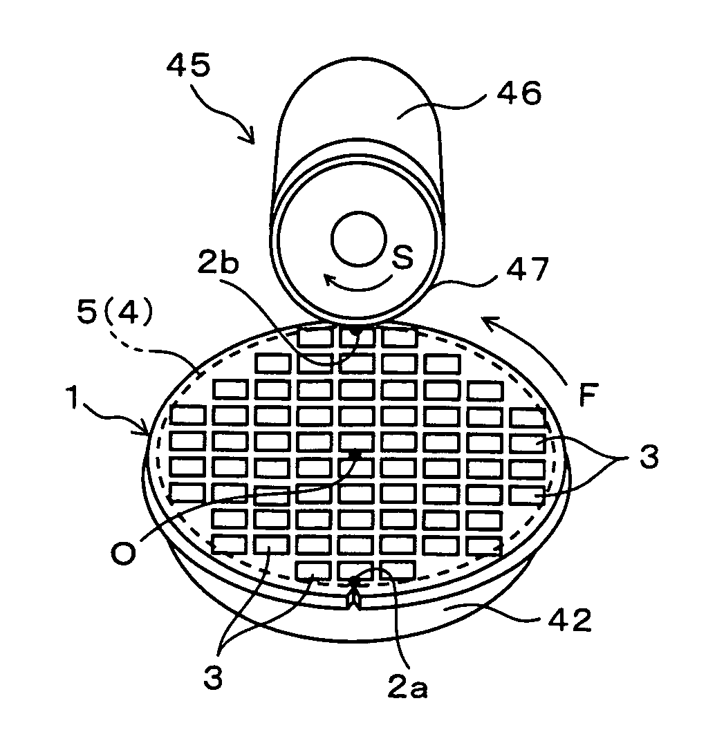
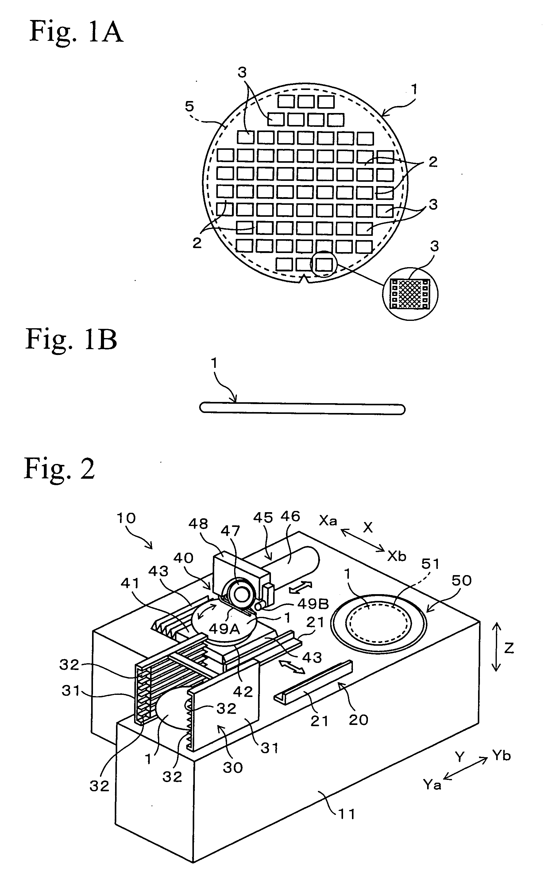
[0033]FIGS. 1A and 1B show a disc-shaped semiconductor wafer 1 (hereinafter referred to simply as “wafer 1”) which is a substrate in the embodiment. The wafer 1 is a silicon wafer or the like and has a thickness of about 600 to 700 μm. Grid-like predetermined division lines 2 are formed on a surface of the wafer 1 so that plural rectangular semiconductor chips 3 are defined by the predetermined division lines 2 on the surface of the wafer 1. Electronic circuits (for example, Integrated Circuits (=ICs) and Large Scale Integrations (=LSIs)) are formed on surfaces of the semiconductor chips 3.

[0034] A rear surface of the wafer 1 is ground so that the wafer 1 is thinned to have a desired thickness (for example, about 50 to 100 μm). Next, the wafer 1 is cut along the predetermined division lines 2 and is divided into the semiconductor chips 3. In the embodi...


PUM


Abstract

A cutting method for substrates includes: preparing a substrate which has a predetermined circular cut line set thereon; chucking the substrate on a surface of a chuck table which is rotatably supported around a rotation axis of the chuck table such that the predetermined circular cut line of the substrate is concentric with the chuck table; disposing a disc-shaped cutting blade having a rotation axis so that the cutting blade faces the substrate; and cutting the substrate along the predetermined circular cut line of the substrate by the cutting blade while rotating the substrate by rotating the chuck table. The substrate has two cut points which are set on one side and the other side of the predetermined circular cut line such that a rotation center of the substrate is positioned between the one side and the other side of the predetermined circular cut line. The cutting blade is disposed so that the rotation axis of the cutting blade perpendicularly crosses the rotation axis of the chuck table. The cutting blade is reciprocatably supported along the rotation axis of the cutting blade, and alternately cuts into the two cut points of the substrate.

Description

[0001] This application claims priority under 35 U.S.C. § 119 to Japanese Patent Application No. JP2005-355078 filed Dec. 8, 2005, the entire content of which is hereby incorporated by reference. BACKGROUND OF THE INVENTION [0002] 1. Field of the Invention [0003] The present invention relates to a cutting method for substrates (for example, semiconductor wafers) in which a substrate is circularly cut by using a cutting blade and a groove is formed on a substrate by using it. The present invention relates to a cutting apparatus which is advantageously used for the cutting method. [0004] 2. Description of Related Art [0005] Semiconductor devices (for example, semiconductor chips) are produced by the following processes. That is, a wafer (for example, a semiconductor wafer) which is composed of a semiconductor substrate material is prepared. Grid-like predetermined division lines are formed on a surface of the wafer, so that plural rectangular device regions are defined by the predeter...

Claims


Application Information

Patent Timeline
Patent Type & Authority Applications(United States)
IPC IPC(8): H01L21/00
CPCH01L21/67092
Inventor WATANABE, SHINYA
Owner DISCO CORP
Why Eureka
Try Eureka