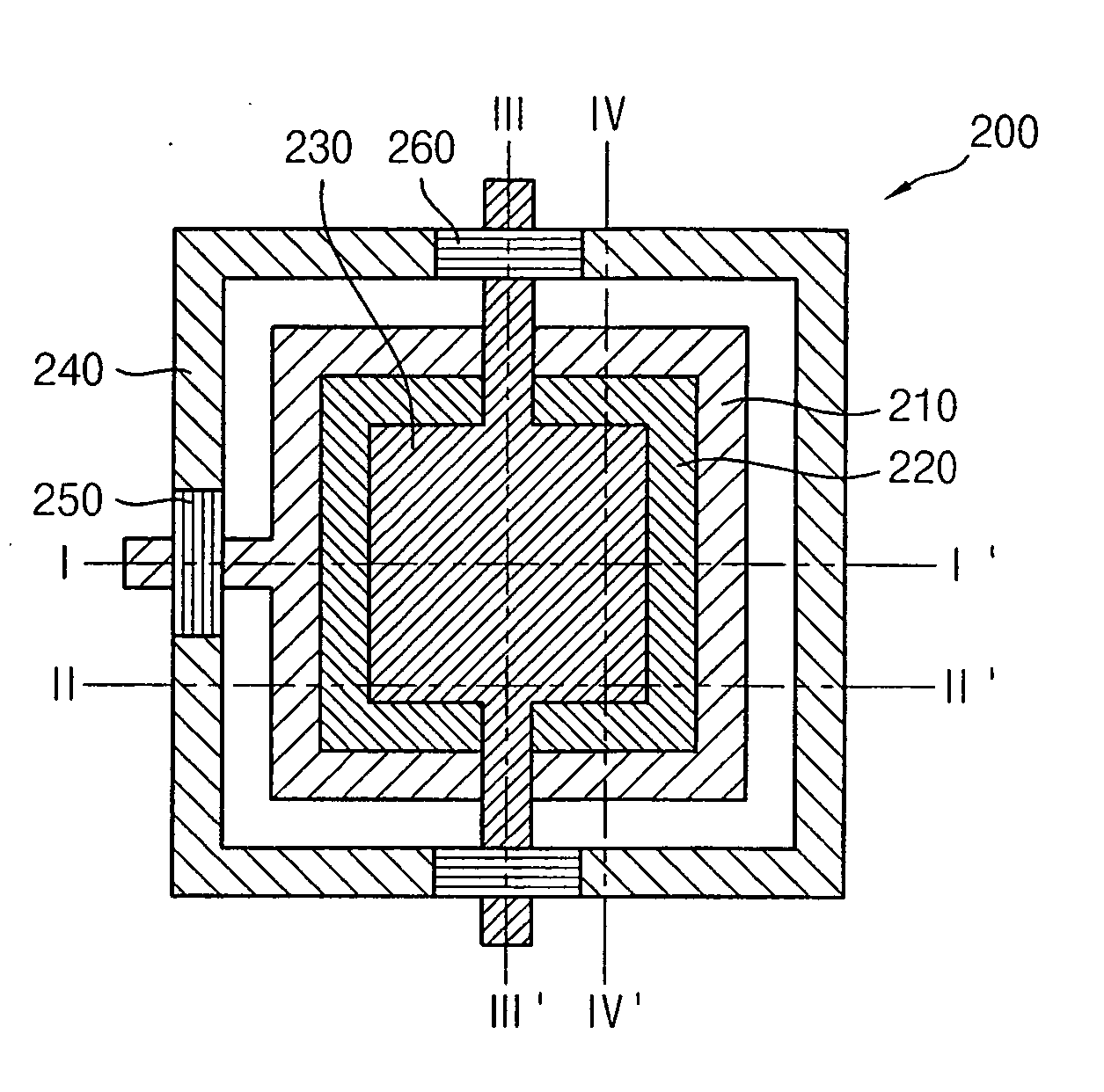
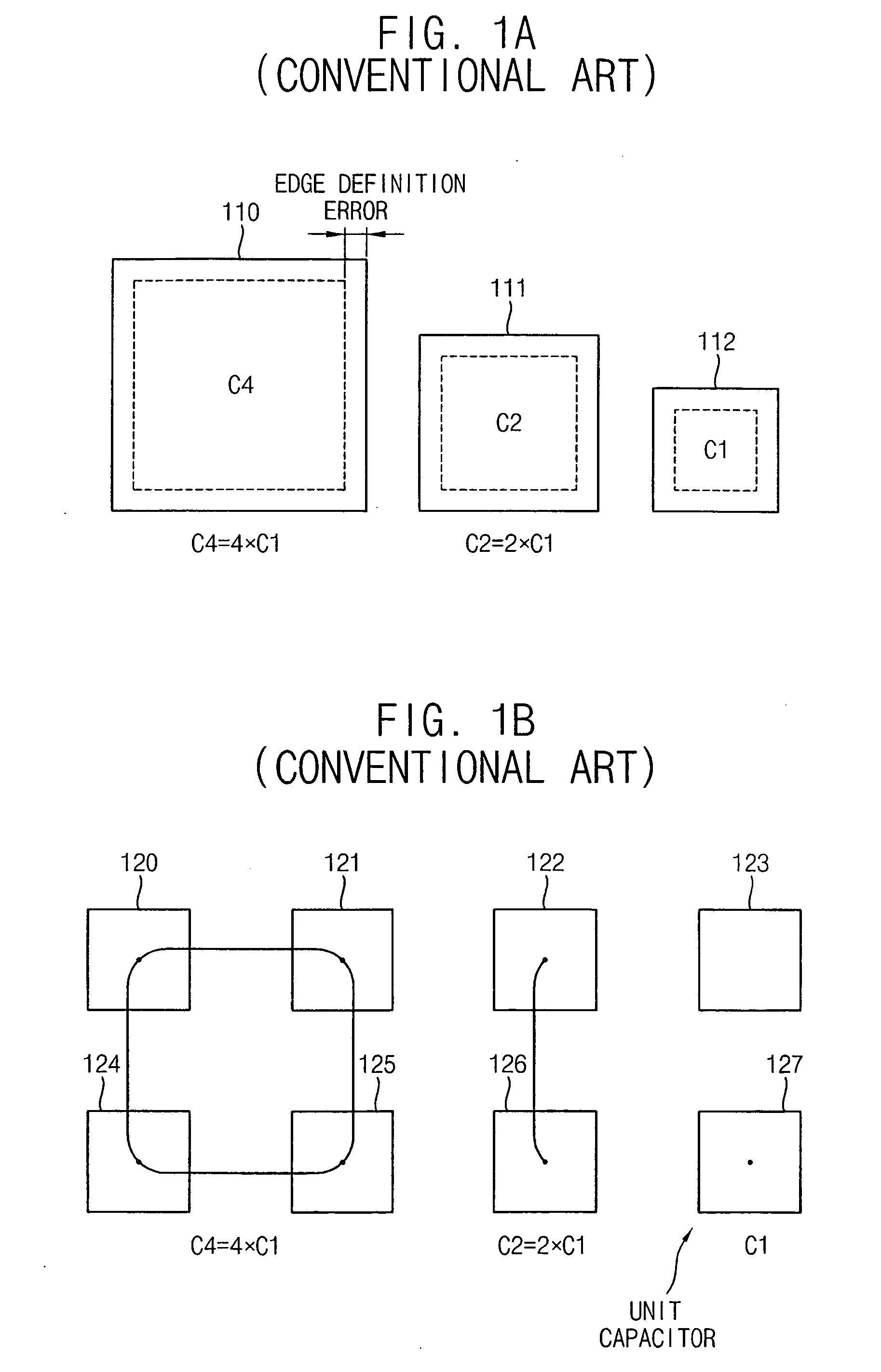
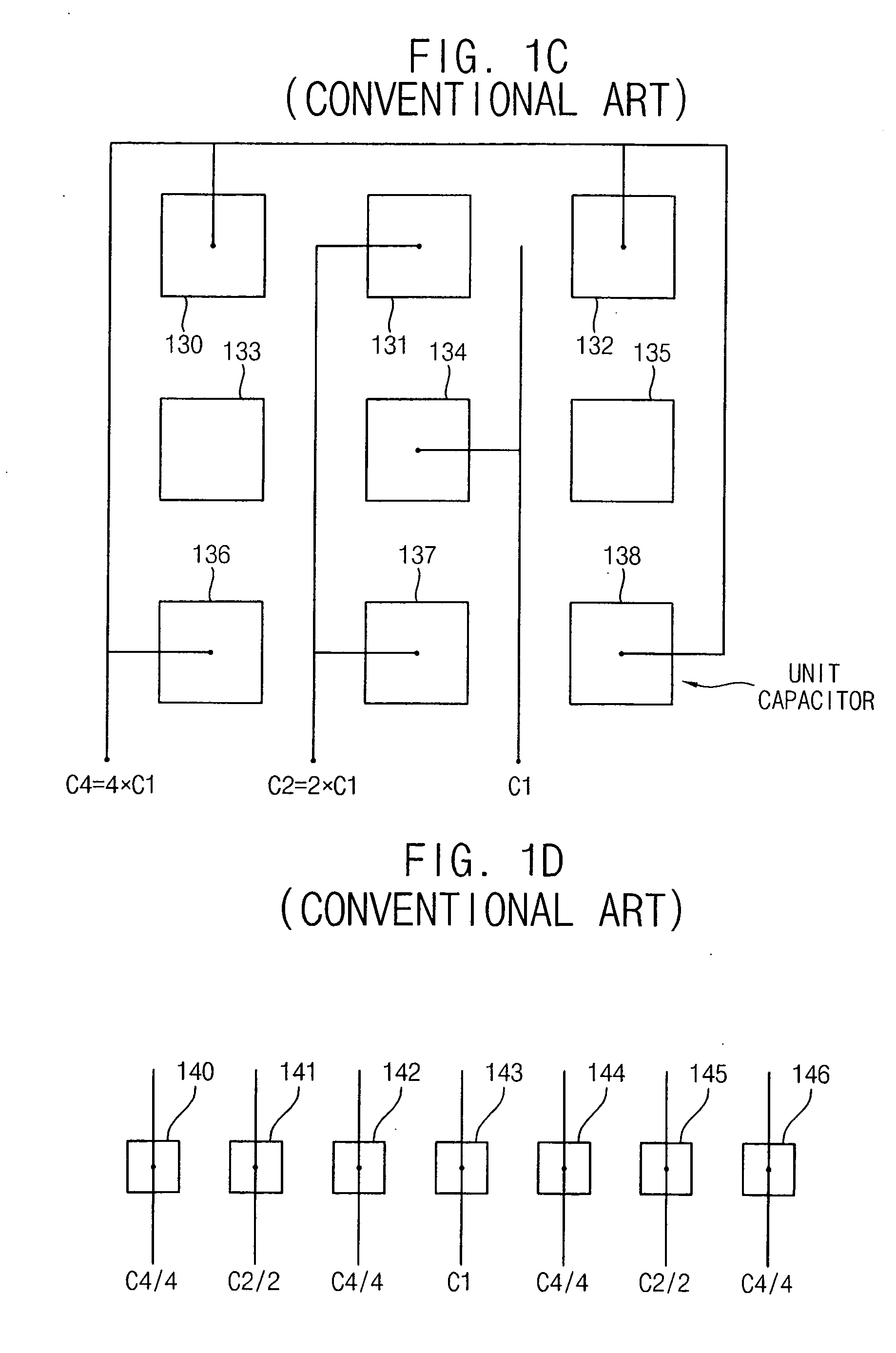
Capacitor and capacitor array
a capacitor array and capacitor technology, applied in the field of capacitor arrays, can solve the problems of precision limitation, the approach to make the capacitor array of binary-weighted ladders shown in fig. 1a cannot be used in precise adcs, and limit the manufacturing process, so as to reduce the parasitic capacitance
- Summary
- Abstract
- Description
- Claims
- Application Information
AI Technical Summary
Benefits of technology
Problems solved by technology
Method used
Image

Examples
Embodiment Construction
[0052] It will be understood that, although the terms first, second, etc. can be used herein to describe various elements, these elements should not be limited by these terms. These terms are only used to distinguish one element from another. For example, a first element could be termed a second element, and, similarly, a second element could be termed a first element, without departing from the scope of the present invention. As used herein, the term “and / or” includes any and all combinations of one or more of the associated listed items.
[0053] It will be understood that when an element is referred to as being “on” or “connected,” or “coupled” to another element, it can be directly on or connected or coupled to the other element or intervening elements can be present. In contrast, when an element is referred to as being “directly on” or “directly connected” or “directly coupled” to another element, there are no intervening elements present. Other words used to describe the relatio...
PUM
 Abstract
Description
Claims
Application Information
 - R&D
- Intellectual Property
- Life Sciences
- Materials
- Tech Scout
- Unparalleled Data Quality
- Higher Quality Content
- 60% Fewer Hallucinations
Browse by: Latest US Patents, China's latest patents, Technical Efficacy Thesaurus, Application Domain, Technology Topic, Popular Technical Reports.
© 2025 PatSnap. All rights reserved.Legal|Privacy policy|Modern Slavery Act Transparency Statement|Sitemap|About US| Contact US: help@patsnap.com