Portable scanning electron microscope

a scanning electron microscope and portable technology, applied in the field of scanning electron microscopes, can solve the problems of affecting the scanning effect of the scanning wafer, the cost, complexity and reliability of the moving stage, and the cost of manufacturing,

Inactive Publication Date: 2007-06-28
KLA TENCOR TECH CORP
View PDF33 Cites 19 Cited by
  • Summary
  • Abstract
  • Description
  • Claims
  • Application Information

AI Technical Summary

Benefits of technology

[0012]Another embodiment relates to a portable scanning electron microscope (SEM) apparatus. The apparatus includes at least an SEM column, a vacuum pump coupled to the SEM column, a sample holder, and a rack-and-pinion stage. The rack-and-pinion stage is configured to control movement between an SEM column and a sample holder.

Problems solved by technology

The conventional technique for positioning a region of interest has disadvantages relating to cost, complexity and reliability of the moving stage.
In addition, the conventional technique may have a relatively slow throughput rate for scanning wafers due to the need to reposition (or continuously move) the wafer under the beam.
The large bulk of the conventional apparatus makes it costly to manufacture and also limits its practical applications.
For example, the large bulk of the stage makes it difficult to integrate the inspector into another semiconductor equipment tool for in-situ metrology applications.

Method used


Image

  • Portable scanning electron microscope
  • Portable scanning electron microscope
  • Portable scanning electron microscope

Examples


Embodiment Construction

[0031]Electron Microscope Apparatus Using CRT-Type Optics

[0032]Traditional optical methods are available for macro wafer inspection, but these optical methods are not sensitive to electrical properties. Electron beam (e-beam) inspection tools are available, but these tools are currently too slow to be practical for wafer-level mapping on the order of several to tens of wafers per hour. Furthermore, vibrations in conventional e-beam inspection tools causes degradation of image resolution.

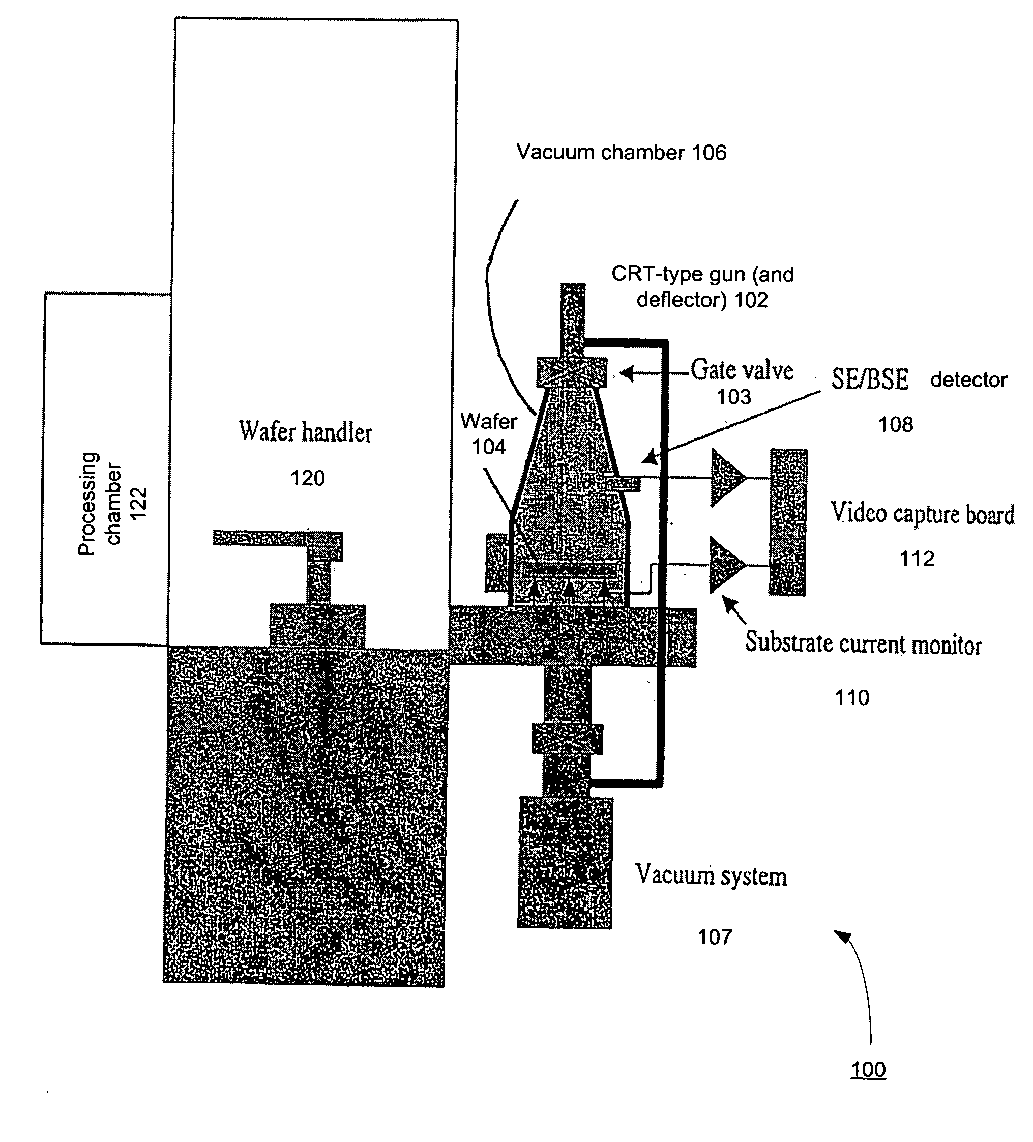
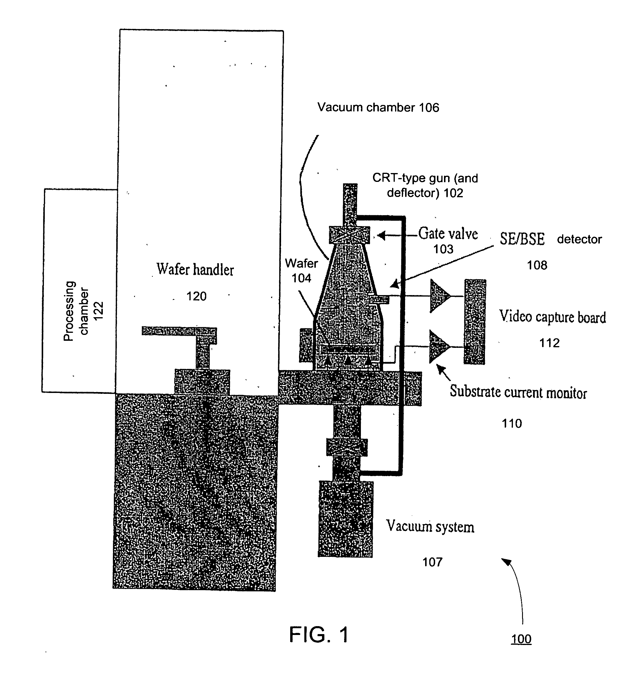
[0033]FIG. 1 is a schematic diagram of a high-speed two-dimensional scanning apparatus 100 for automated electron beam inspection in accordance with an embodiment of the invention. The two-dimensional scanning apparatus 100 is configured to advantageously utilize a cathode ray tube (CRT)-type gun (and deflection) 102 technology. The two-dimensional scanning apparatus 100 may be called a “macro” e-beam inspector with CRT-type optics.

[0034]In one embodiment, a wafer handler 120 may retrieve the wafer f...


PUM


Abstract

One embodiment relates to a portable scanning electron microscope (SEM) system. The system includes a portable SEM device including a CRT-type gun and deflectors to generate and scan the electron beam. Another embodiment relates to a portable SEM device which includes a CRT-type gun and deflectors to generate and scan the electron beam, a chamber through which the electron beam is scanned, and a detector in the chamber for detecting radiation emitted as a result of scanning the electron beam. Another embodiment relates to a method of obtaining an electron beam image of a surface of a bulk specimen where a portable SEM device is moved to the bulk specimen. Other embodiments and features are also disclosed.

Description

CROSS-REFERENCE TO RELATED APPLICATION[0001]The present application claims the benefit of U.S. Provisional Patent Application No. 60 / 772,155, entitled “Portable Scanning Electron Microscope,” filed Feb. 10, 2006, by inventors David L. Adler and Ady Levy, the disclosure of which is hereby incorporated by reference. The present application claims the benefit of U.S. Provisional Patent Application No. 60 / 749,868, entitled “Electron Microscope Apparatus Using CRT-Like Optics,” filed Dec. 12, 2005, by inventors Avi Cohen, David L. Adler and Neil Richardson, the disclosure of which is hereby incorporated by reference. The present application is related to U.S. patent application Ser. No. 11 / 031,091, entitled “High-Speed Electron Beam Inspection,” filed Jan. 6, 2005, by inventors David L. Adler, et al., the disclosure of which is also hereby incorporated by reference.BACKGROUND OF THE INVENTION[0002]1. Field of the Invention[0003]The present disclosure relates to scanning electron microsco...

Claims


Application Information

Patent Timeline
Patent Type & Authority Applications(United States)
IPC IPC(8): G21K7/00
CPCH01J37/04H01J37/06H01J37/228H01J37/28H01J2237/04924H01J2237/06316H01J2237/162H01J2237/2813
Inventor ADLER, DAVID L.LEVY, ADYMCCORD, MARK A.
Owner KLA TENCOR TECH CORP
Why Eureka
Try Eureka