
Analog frequency divider

a frequency divider and analog technology, applied in the field of analog frequency dividers, can solve the problems of power consumption increase, inability to perform frequency dividing operation, and loss of amplification circuit gain in an rf frequency band, so as to achieve easy formation, increase resistance value, and extend the frequency band of the operation of the frequency divider.

Inactive Publication Date: 2007-06-28
TOYOTA IND CORP
View PDF7 Cites 1 Cited by
  • Summary
  • Abstract
  • Description
  • Claims
  • Application Information

AI Technical Summary

Benefits of technology

[0011] According to the present invention, the operational frequency band of a frequency divider can be extended by using the parallel circuit of an inductor and a resistor as the load of the first, second, seventh and eighth MOS transistors. Since the load is made of the parallel circuit of an inductor and a resistor, the resistance value can be increased compared with the series circuit of an inductor and a resistor. By increasing the resistance value, the Q value of the analog frequency divider can be prevented from varying due to the dispersion of the resistance value. More particularly, if an analog frequency divider is formed on a semiconductor device, the device area of a resistor needed to realize a necessary resistance value can be reduced since the resistance value can be fairly easily formed on the semiconductor device.

Problems solved by technology

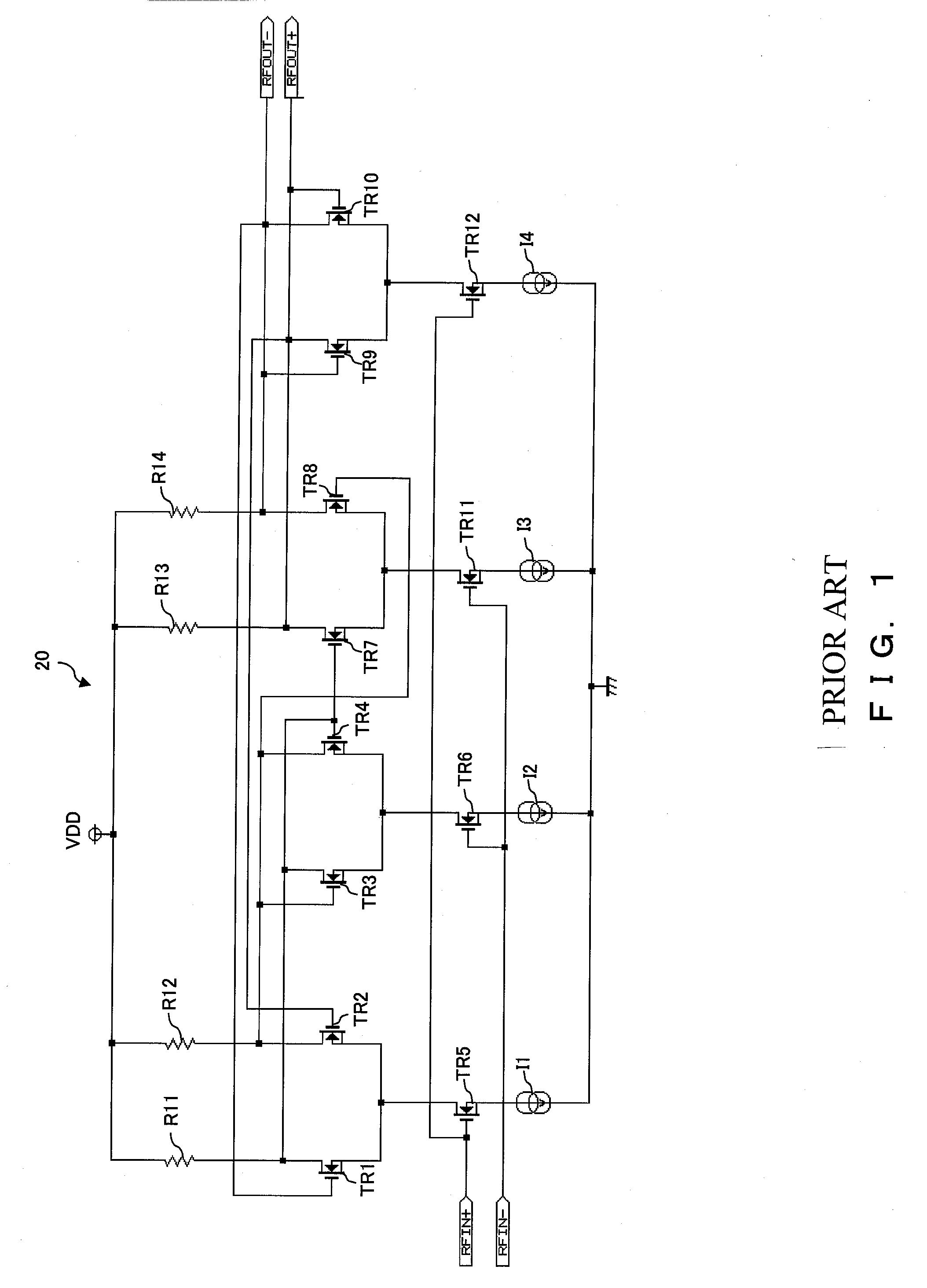
The conventional analog frequency divider 20 has a problem that the gain of the amplification circuit decreases in an RF frequency band and the frequency dividing operation is impossible since resistors are used as the load of MOS transistors TR1, TR2, TR7 and TR8.
As a result, power consumption increases.
However, if the resistance value is small, the resistance value varies widely, which greatly affects the Q value of the frequency divider.

Method used


Image

  • Analog frequency divider
  • Analog frequency divider
  • Analog frequency divider

Examples


Embodiment Construction

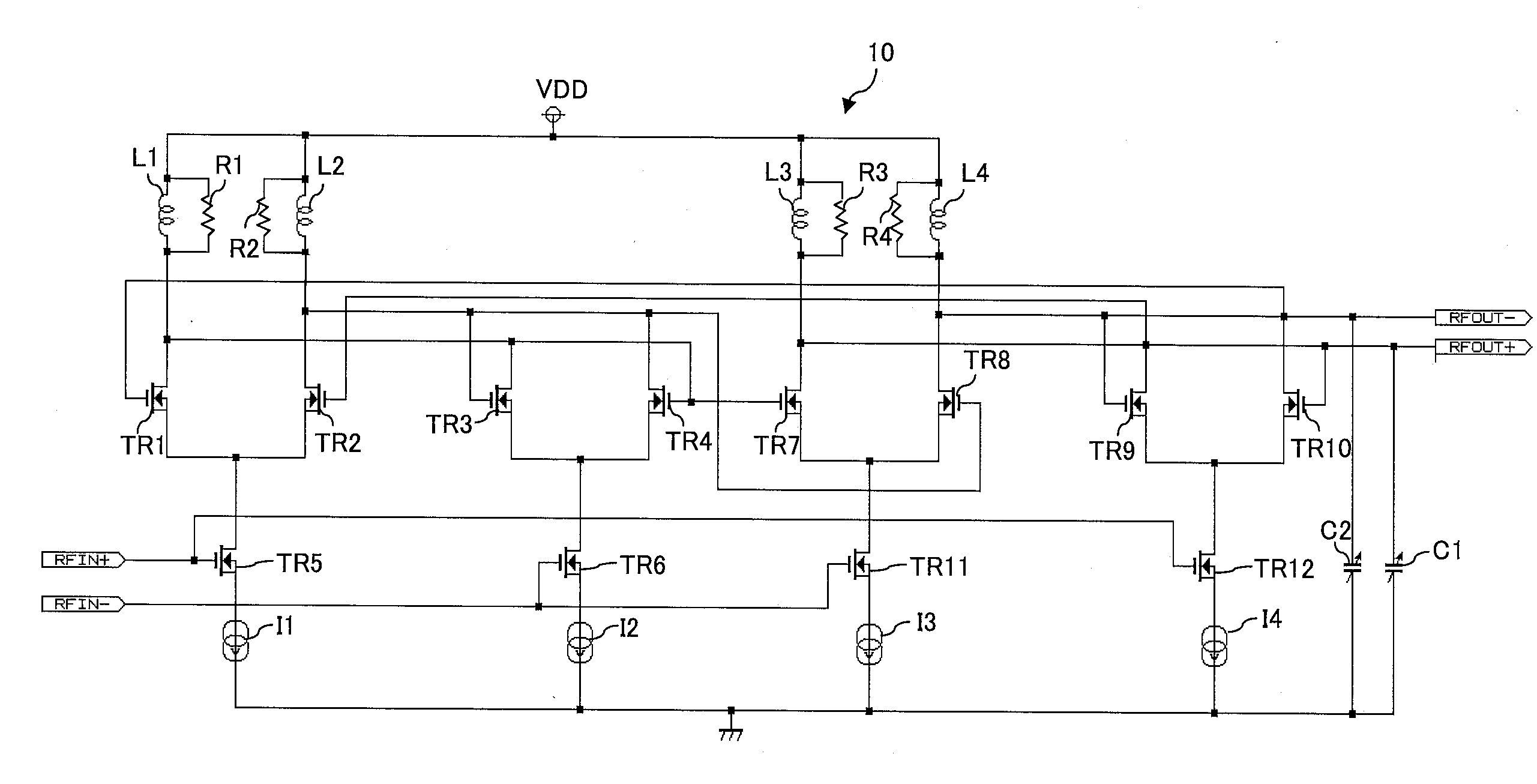
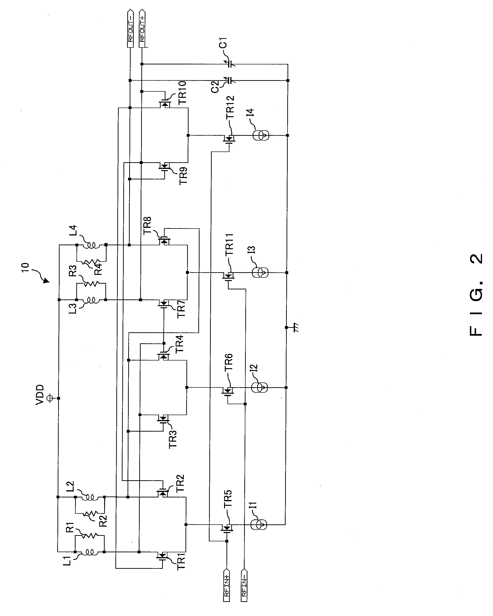
[0019] The preferred embodiments are described below with reference to the drawings. FIG. 2 shows the circuit diagram of the analog frequency divider of the preferred embodiment. This analog frequency divider is formed, for example, on a semiconductor device manufactured in a MOS process.

[0020] An analog frequency divider 10 is used, for example, in an RF frequency band of 5 GHz or more. To the analog frequency divider, an RFIN+ signal (corresponding to an input signal P) and its inverted signal RFIN− (corresponding to an inverted signal N) are inputted. The input signal RFIN+ and the inverted signal RFIN− are, for example, the output signal of a voltage controlled oscillator (VCO) and a signal obtained by inverting the output signal.

[0021] In the analog frequency divider 10 shown in FIG. 2, an amplifier for amplifying input signals RFIN+ and RFIN− and a latch unit are connected in two stages, and has a function to divide the input signals RFIN+ and RFIN− respectively in half in f...


PUM


Abstract

The parallel circuit of an inductor L1 and a resistor R1 is connected between a power supply voltage VDD and the drain of a MOS transistor TR1 as a load, and the parallel circuit of am inductor L2 and a resistor R2 is connected between a power supply voltage VDD and the drain of a MOS transistor TR2 as a load.

Description

CROSS REFERENCE TO RELATED APPLICATIONS [0001] This application claims priority to Japanese Patent Application No. 2005-365298 Dec. 19, 2005. FIELD OF THE INVENTION [0002] The present invention relates to an analog frequency divider used in an RF frequency band. BACKGROUND OF THE INVENTION [0003] Conventionally, the circuit shown in FIG. 1 is used for an analog frequency divider. In the analog frequency divider 20 shown in FIG. 1, two stages of flip-flop circuits each composed of an amplifier for amplifying signals and a latch unit for maintaining the output state of the amplifier is connected. [0004] The amplifier of the first stage flip-flop circuit comprises MOS transistors TR1, TR2 and TR5 and a current source 11 and its latch unit comprises MOS transistors TR3, TR4 and TR6 and a current source 12. The amplifier of the second stage flip-flop circuit comprises MOS transistors TR7, TR8 and TR11 and a current source 13 and its latch unit comprises MOS transistors TR9, TR10 and TR12...

Claims


Application Information

Patent Timeline
Patent Type & Authority Applications(United States)
IPC IPC(8): H03K23/00
CPCH03K23/60
Inventor INOUE, JUNJI
Owner TOYOTA IND CORP
Learn More