This helps you quickly interpret patents by identifying the three key elements:
Problems solved by technology
Method used
Benefits of technology
Benefits of technology
[0012] Therefore, an object of the present invention is to reduce the number of image signal lines for connecting a driver IC with a liquid crystal display portion and display a preferable image.
[0039] According to the present invention, the scanning signal line is dynamically connected between a source which supplies the scanning signal and a pixel line which is a portion to which the scanning signal is supplied. Therefore, the number of signal lines connected between a driver IC and a liquid crystal display portion can be reduced and a preferable image can be displayed.
Image
Click on the blue label to locate the original text in one second.
Reading with bidirectional positioning of images and text.
Examples
modified example 1
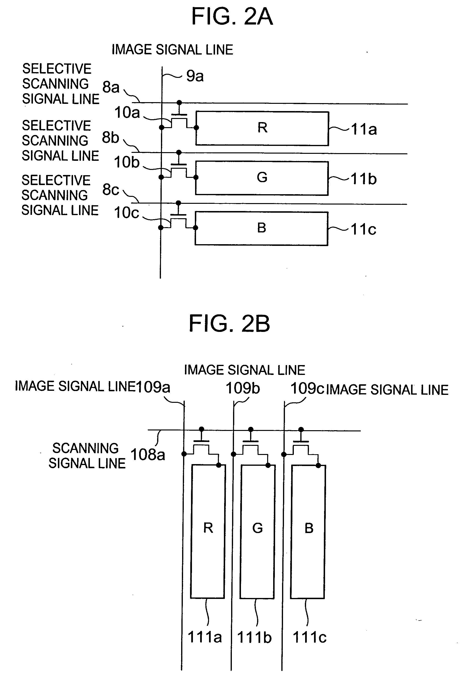
[0159] Next, Modified Example 1 will be described. In this modified example, a pixel line group (pixel line set) is formed for each group including the color pixel lines corresponding to, R, G, and B, that is, the three primary colors.
[0160] In the image display device 1, the same image signal line 9 is connected with pixels 11 corresponding to R, G, and B. Therefore, when the liquid crystal display portion 5 is scanned in a direction from an upper end to a lower end (or reverse direction) in order, the signal traveling on the image signal line 9 is switched to one of the image signal of R, the image signal of G, and the image signal of B every time the scanning signal moves from a pixel line to next pixel line.
[0161] Therefore, the image signal traveling on the image signal line 9 significantly varies, so there may occur an inconvenience such as a crosstalk.
[0162] The liquid crystal display portion 5 is not necessarily scanned from the upper end to the lower end in order. Scanni...
modified example 2
[0188] In this modified example, the group of each of R, G, and B is divided into an even group and an odd group, with the result that the groups of R, G, and B are divided into six groups. To be specific, the pixel lines of R are divided into an even-numbered pixel line group and an odd-numbered pixel line group which are counted from the uppermost line. The pixel lines of G are divided into an even-numbered pixel line group and an odd-numbered pixel line group. The pixel lines of B are divided into an even-numbered pixel line group and an odd-numbered pixel line group.
[0189] For example, in an example shown in FIG. 9, the pixel 11a is assumed to belong to an even-numbered pixel line of the pixel lines of R and is included in the first group.
[0190] Similarly, the pixel 11b is assumed to belong to an even-numbered pixel line of the pixel lines of G and is included in the second group. In addition, the pixel 11c is assumed to belong to an even-numbered pixel line of the pixel lines...
PUM
Abstract
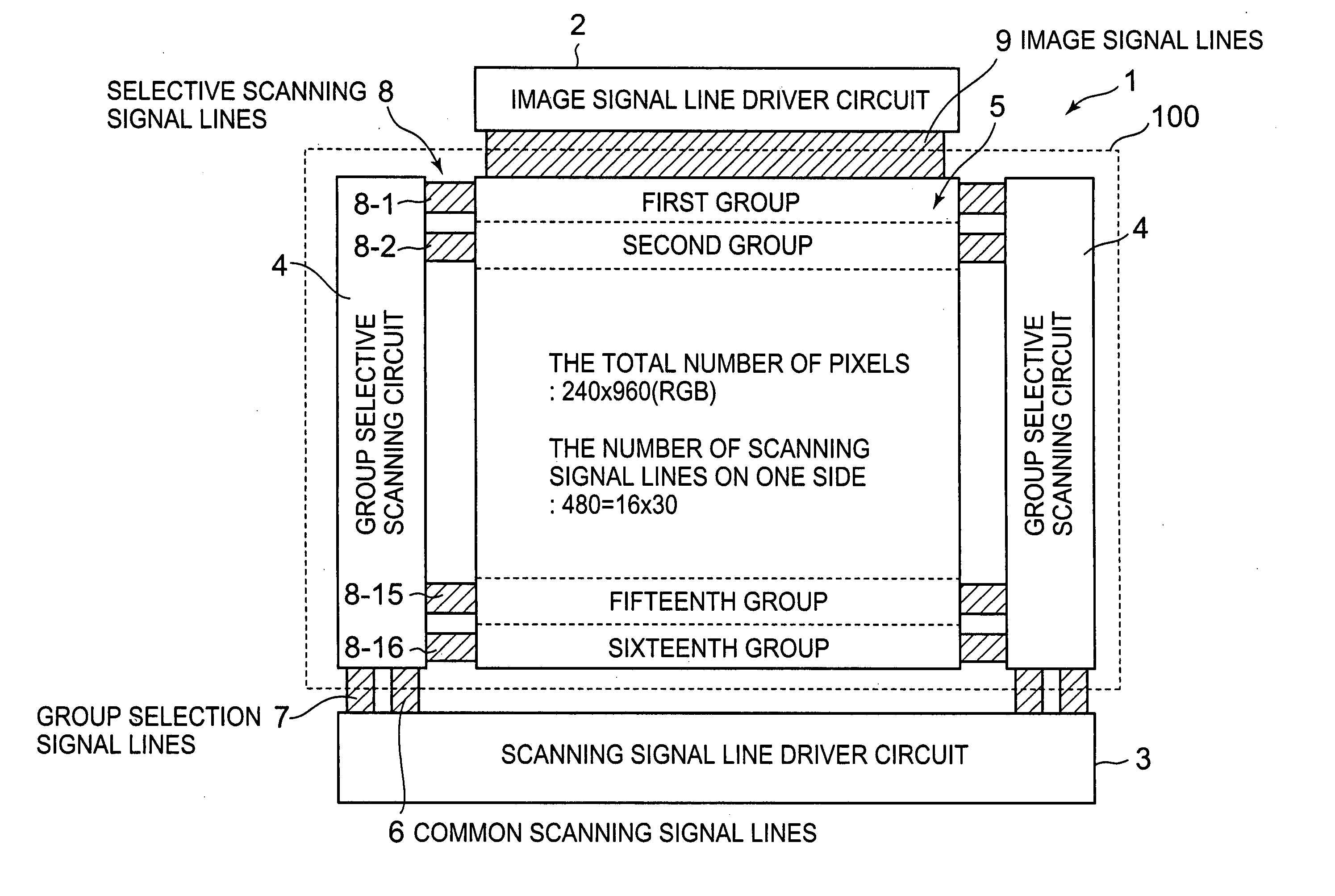
Provided are an image display device and an image display method capable of reducing the number of signal lines connected between a driver IC and a liquid crystal display portion and of displaying a preferable image. A liquid crystal display portion is divided into 16 division groups in a scanning direction. In order to scan the liquid crystal display portion, a common scanning signal line which is a scanning signal output line of a scanning signal line driver circuit is connected with a selective scanning signal line of each of the 16 division groups during switching for each of the groups. The common scanning signal line is commonly used among the plurality of selective scanning signal lines, so the number of wirings to be connected in the driver IC can be reduced.
Description
[0001] This application claims priority under 35 U.S.C. § 119 to Japanese Patent Application Nos. JP 2005-348401, filed Dec. 1, 2005, and JP 2006-310391, filed Nov. 16, 2006, the entire content of which is hereby incorporated by reference. BACKGROUND OF THE INVENTION [0002] 1. Field of the Invention [0003] The present invention relates to an image display method and an image display device such as an active matrixliquid crystal display device including switching elements. [0004] 2. Description of the Related Art [0005] A liquid crystal display device is thin and has lower power consumption. Therefore, the liquid crystal display device has been widely used as a display of, for example, a television receiver, a computer, or a mobile telephone. [0006] There are various types of liquid crystal display devices. An example of a widely used liquid crystaldisplay device is an active matrix liquid crystaldisplay device in which a switching element is provided in each pixel to drive a liqu...
Claims
Application Information
Patent Timeline
Application Date:The date an application was filed.
Publication Date:The date a patent or application was officially published.
First Publication Date:The earliest publication date of a patent with the same application number.
Issue Date:Publication date of the patent grant document.
PCT Entry Date:The Entry date of PCT National Phase.
Estimated Expiry Date:The statutory expiry date of a patent right according to the Patent Law, and it is the longest term of protection that the patent right can achieve without the termination of the patent right due to other reasons(Term extension factor has been taken into account ).
Invalid Date:Actual expiry date is based on effective date or publication date of legal transaction data of invalid patent.

