Method of measuring film thickness and method of manufacturing semiconductor device

a technology of semiconductor devices and film thickness, which is applied in the direction of measurement devices, semiconductor/solid-state device testing/measurement, instruments, etc., can solve the problems of low accuracy of optical film thickness measurement, material with low reflectance, and measurement utilizing metal surface reflection is not applicable to materials having low reflectance. , to achieve the effect of increasing yield and productivity in manufacturing semiconductor devices

Inactive Publication Date: 2007-06-28
FUJITSU SEMICON LTD
View PDF23 Cites 2 Cited by
  • Summary
  • Abstract
  • Description
  • Claims
  • Application Information

AI Technical Summary

Benefits of technology

[0026] Accordingly, yield and productivity in ma

Problems solved by technology

However, there has been no appropriate method for controlling the thickness of insulating films that are formed after ferroelectric memories (FeRAMs) production processes.
Some of the reasons are: that the accuracy of optical film thickness measurements is low due to the complicated structure of films formed on silicon substrates; and that measurements utilizing reflection from metal surfaces are not appli

Method used


Image

  • Method of measuring film thickness and method of manufacturing semiconductor device
  • Method of measuring film thickness and method of manufacturing semiconductor device
  • Method of measuring film thickness and method of manufacturing semiconductor device

Examples


Embodiment Construction

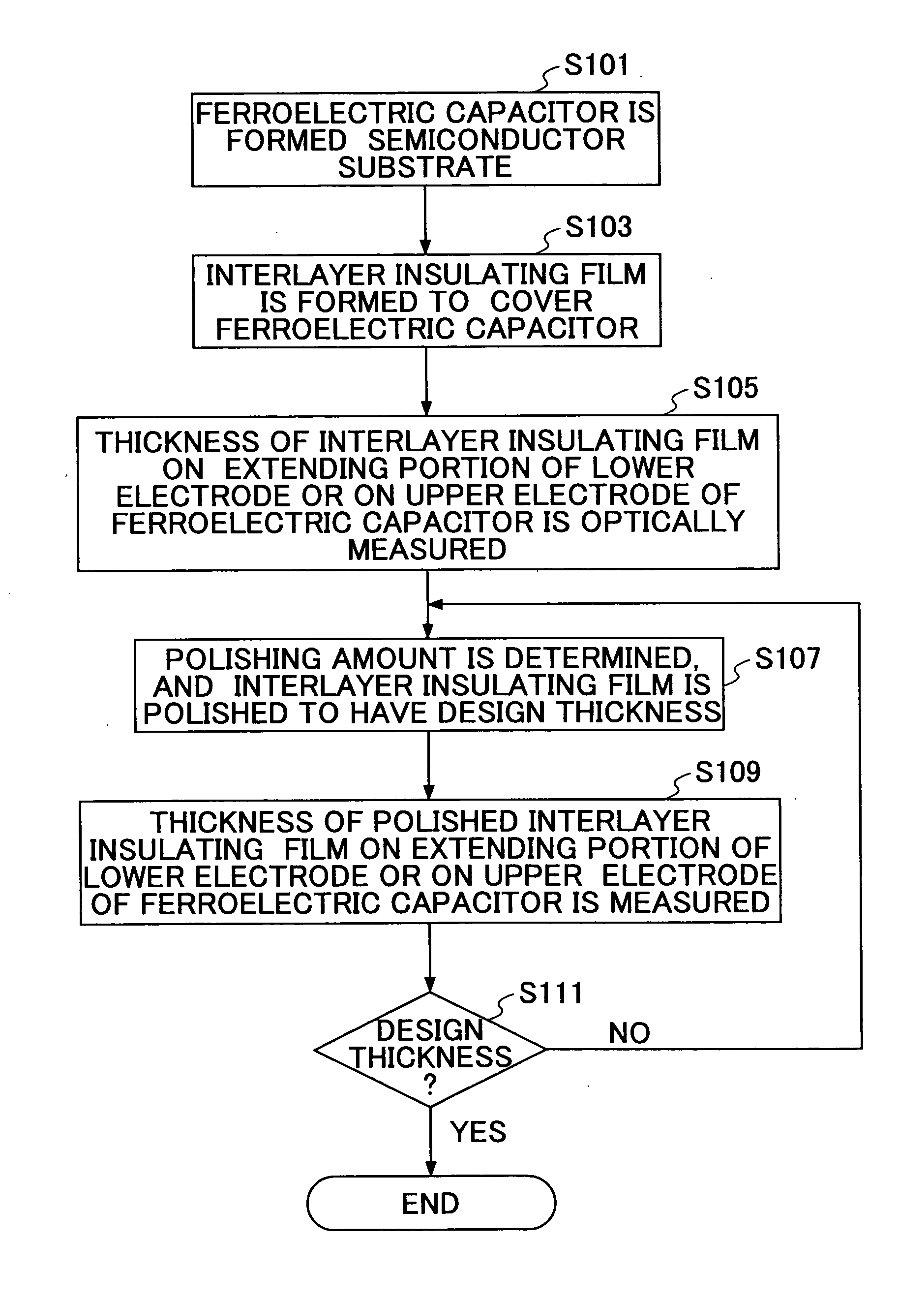
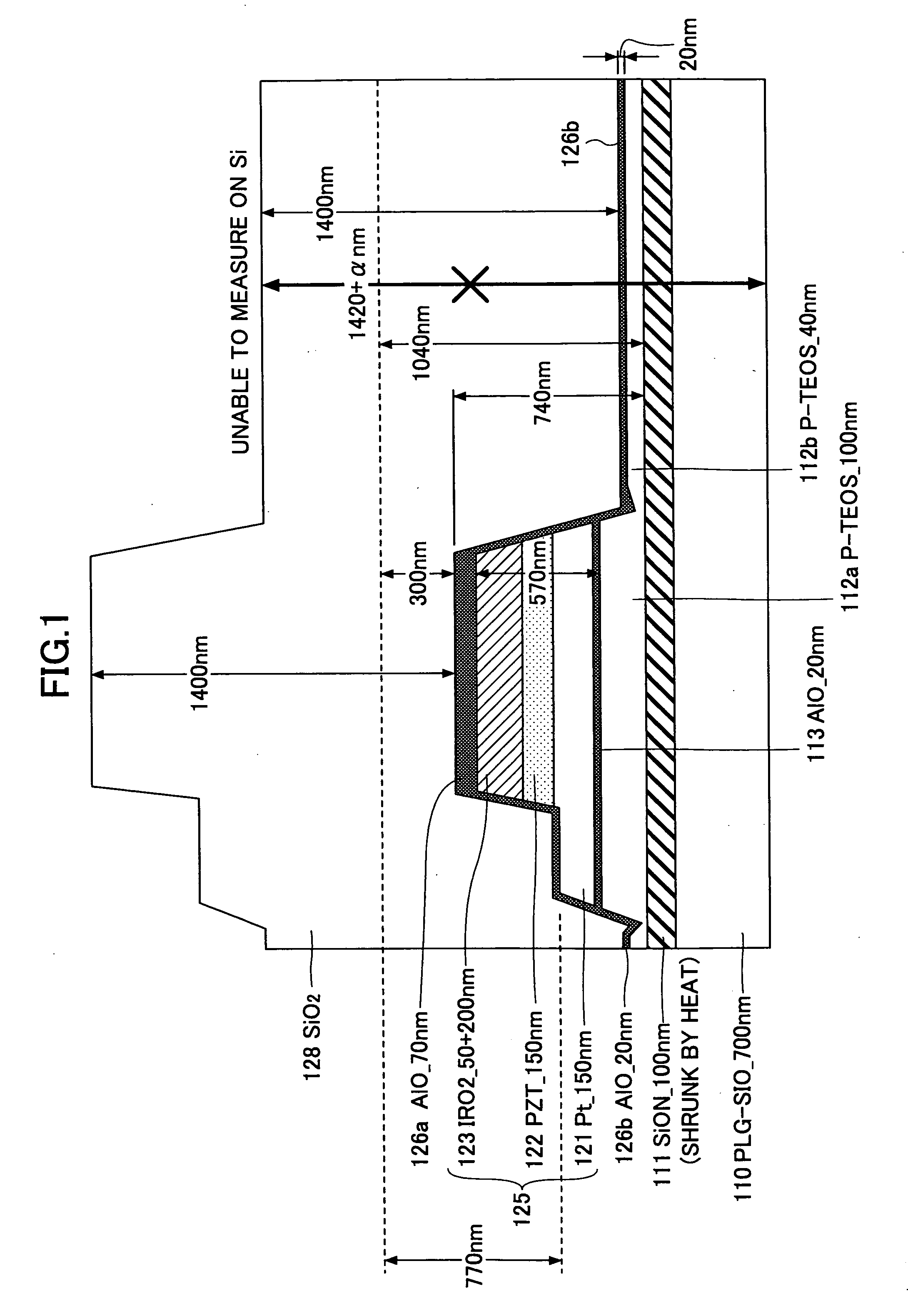
[0034]FIGS. 3 and 4 are cross-sectional views showing an example of a semiconductor device for illustrating a film thickness measuring method according to an embodiment of the present invention.

[0035] Referring to FIG. 3, a first interlayer insulating film 10 of 700 nm thickness is formed to cover a transistor (not shown) on a silicon substrate. A ferroelectric capacitor 25 is formed on the first interlayer insulating film 10, with a SiON cap film 11, a TEOS cap film 12, and an Al2O3 cap film 13 interposed therebetween.

[0036] The ferroelectric capacitor 25 includes a lower electrode 21, a ferroelectric film 22, and an upper electrode 23. The lower electrode 21 is an extraction electrode extending horizontally to be connected to an upper interconnect. The ferroelectric capacitor 25 is entirely covered with an Al2O3 capacitor protecting film (hydrogen diffusion preventing film) 26. It is to be noted that the Al2O3 capacitor protecting film 26 on the upper electrode 23 is denoted by ...


PUM


Abstract

A method of measuring a film thickness is disclosed. The method includes a step of forming a ferroelectric capacitor on a substrate, a step of forming an insulating film to cover the ferroelectric capacitor, and a step of optically measuring the thickness of the insulating film on an electrode of the ferroelectric capacitor.

Description

CROSS-REFERENCE TO RELATED APPLICATIONS [0001] This application is based upon and claims priority of Japanese Patent Application No. 2005-375678, filed on Dec. 27, 2005, the contents being incorporated herein by reference. BACKGROUND OF THE INVENTION [0002] 1. Field of the Invention [0003] The present invention generally relates to a method of measuring film thickness of a semiconductor device, and particularly relates to a film thickness measuring method for use in a process of forming an insulating film after a process of forming a ferroelectric capacitor, and a semiconductor device manufacturing method using the same. [0004] 2. Description of the Related Art [0005] In film forming / polishing processes of semiconductor devices, process management and control based on real time measurement of film thickness is required in order to improve yield and ensure device reliability. Especially, controlling the thickness of films formed on elements by sputtering is important because the film...

Claims


Application Information

Patent Timeline
IPC IPC(8): H01L21/66G01R31/26
CPCH01L22/12H01L22/20
Inventor IZUMI, KAZUTOSHITAKEUCHI, TETSUYA
Owner FUJITSU SEMICON LTD
Why Eureka
Try Eureka