
Method of fabricating circuitry without conductive circle

a technology of circuit board and conductive circle, which is applied in the direction of printed circuits, electrical devices, printed circuit aspects, etc., can solve the problems of design and layout, limit the degree of miniaturization of circuit boards,

Inactive Publication Date: 2007-06-28
GOLD CIRCUIT ELECTRONICS
View PDF2 Cites 2 Cited by
  • Summary
  • Abstract
  • Description
  • Claims
  • Application Information

AI Technical Summary

Benefits of technology

[0009] The main objective of the present invention is to provide a method of fabricating circuitry without conductive circles, which has the following advantages:
[0010] 1. Separately processing the two surfaces allows conventional electroplating techniques to be applied with precision to protect the copper layer in the apertures.
[0011] 2. No-conductive circle design eliminates the requirement for alignment of through holes with exposure locations, and facilitates the layout design on the circuit board.
[0012] 3. Localized electroplating means is capable of protecting the copper layer in the apertures, which prevents damage to the copper layer in the etching process, and can also effectively manage some thin-line circuitry.

Problems solved by technology

However, the conductive circles limit circuit design and layout, which in turn limits the degree of miniaturization possible for a circuit board.

Method used


Image

  • Method of fabricating circuitry without conductive circle
  • Method of fabricating circuitry without conductive circle
  • Method of fabricating circuitry without conductive circle

Examples


Embodiment Construction

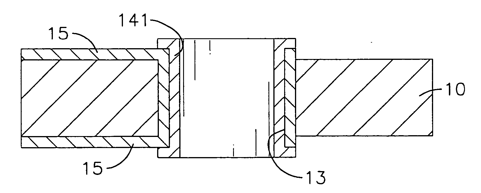
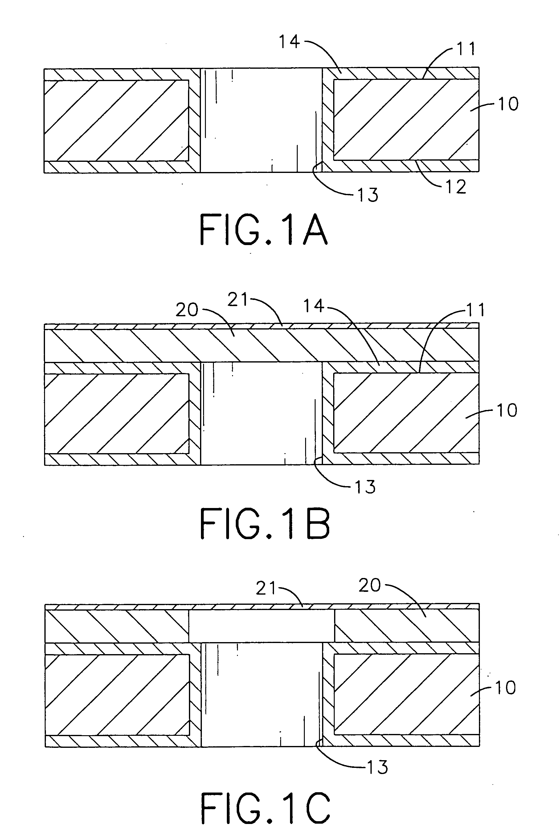
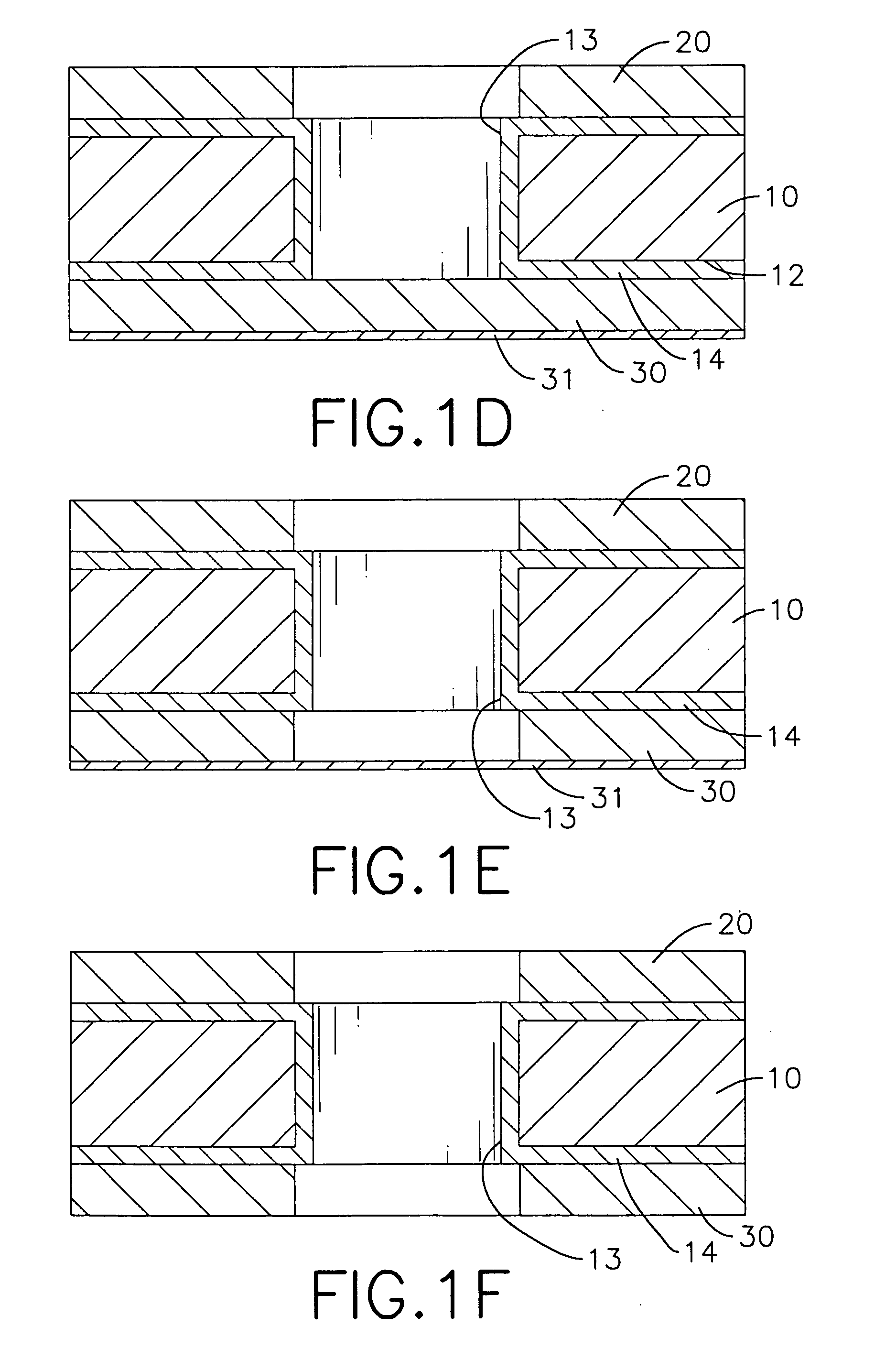
[0017] With reference to FIGS. 1A to 1I, a method of fabricating circuitry on a circuit board comprises the following steps:

[0018] A plate (10) is provided having a first surface (11), a second surface (12) and multiple apertures (13) defined through the first surface (11) and the second surface (12). The first surface (11), the second surface (12) and the inner walls of the apertures (13) are coated with a copper layer (14), as shown in FIG. 1A.

[0019] A first photoresist layer (20) is coated on the copper layer (14) of the first surface (11), and a first protective film (21) is spread over the first photoresist layer (20), as shown in FIG. 1B.

[0020] The first photoresist layer (20) is partly removed at the apertures (13) by exposing, developing and dissolving the photoresist. The apertures (13) are then cleaned and dried, as shown in FIG. 1C. The first protective film (21) is removed from the first photoresist layer (20).

[0021] A second photoresist layer (30) is coated on the c...


PUM


Abstract

A method of fabricating circuitry without conductive circles has steps of providing a plate with multiple apertures defined therein, the plate and inner walls of the apertures are coated with a copper layer; the copper layers are coated with a photoresist layer, which is then covered with a protective film; partly removing the photoresist layer at the apertures; removing the protective film to expose the photoresist layer; electroplating the inner walls of the apertures with copper; exposing and developing the photoresist layers; and finally, etching the copper layers to form a circuit pattern without any conductive circles.

Description

BACKGROUND OF THE INVENTION [0001] 1. Field of the Invention [0002] The present invention relates to a method of fabricating a circuit board, and particularly relates to a method of fabricating circuitry on a circuit board without conductive circles. [0003] 2. Description of the Related Art [0004] A conventional circuit board often has multiple through holes defined therein, and around each through hole, a conductive circle is formed, whereby pins of electrical components are inserted through the holes and soldered to the conductive circle to be electrically connected with the circuitry. [0005] At present, the trend in circuit board design is towards miniaturization. With the development of smaller and smaller electronic products the circuitry involved is required to be accordingly miniaturized. However, the conductive circles limit circuit design and layout, which in turn limits the degree of miniaturization possible for a circuit board. [0006] With reference to FIGS. 2A˜2F, a conv...

Claims


Application Information

Patent Timeline
IPC IPC(8): H01L21/44
CPCH05K3/062H05K3/243H05K3/427H05K2201/09545
Inventor LIN, TING-HAOLEE, CHIH-WEI
Owner GOLD CIRCUIT ELECTRONICS
Learn More