Multi-bit phase-change random access memory (PRAM) with diameter-controlled contacts and methods of fabricating and programming the same

a random access memory and multi-bit technology, applied in the field of pram, can solve the problems of low programming reliability, high programming error, and difficult programming of device types

Inactive Publication Date: 2007-07-05
SAMSUNG ELECTRONICS CO LTD
View PDF13 Cites 22 Cited by
  • Summary
  • Abstract
  • Description
  • Claims
  • Application Information

AI Technical Summary

Benefits of technology

[0012]According to a first aspect, the present invention is directed to a phase-change random-access memory (PRAM) device. The device includes a chalcogenide element, the chalcogenide element comprising a material which can assume a crystalline state or an amorphous state upon application of a heating current. A first contact is connected to a first region of the chalcogenide element and has a first cross-sectional area. A second contact is connected to a second region of the chalcogenide element and has a second cross-sectional area. A first programmable volume of the chalcogenide material is defined in the first region of the chalcogenide element, a state of the first programmable volume being programmable according to a resistance associated with the first contact. A second programmable volume of the chalcogenide material is defined in the second region of the chalcogenide element, a state of the second programmable volume being programmable according to a second resistance associated with the second contact.

Problems solved by technology

In practice, however, this type of device is very difficult to program.
The volume fraction cannot be accurately controlled through the programming process, resulting in very high programming error and, as a result, very low programming reliability.

Method used


Image

  • Multi-bit phase-change random access memory (PRAM) with diameter-controlled contacts and methods of fabricating and programming the same
  • Multi-bit phase-change random access memory (PRAM) with diameter-controlled contacts and methods of fabricating and programming the same
  • Multi-bit phase-change random access memory (PRAM) with diameter-controlled contacts and methods of fabricating and programming the same

Examples


Embodiment Construction

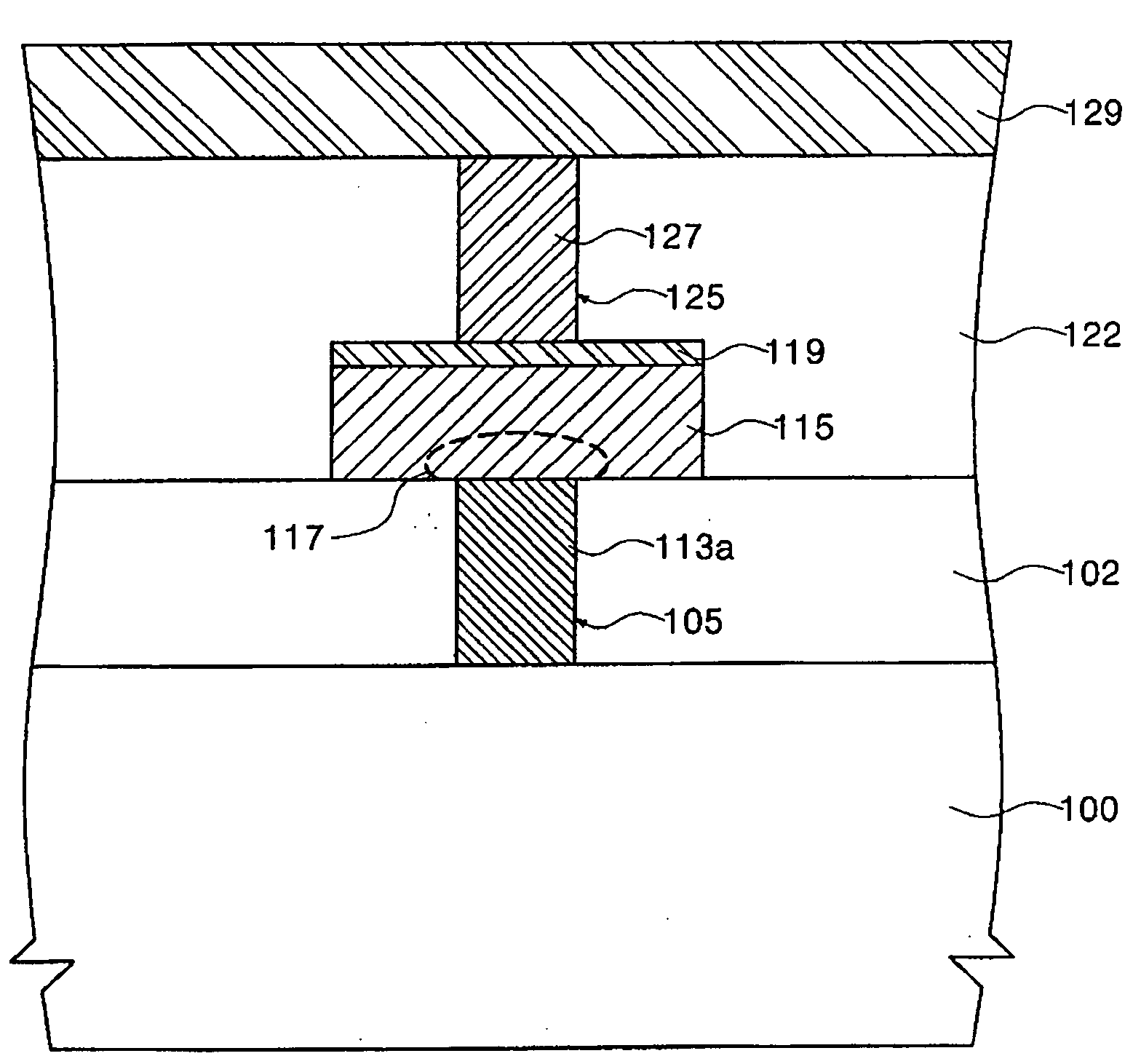
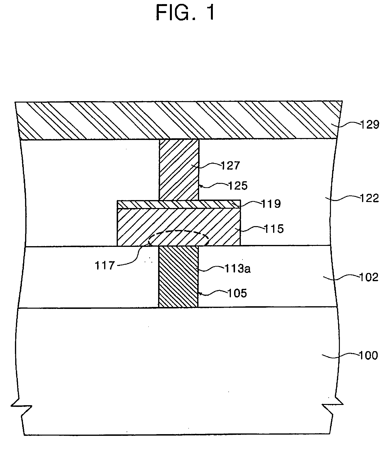
[0049]A semiconductor device and method according to the present invention will now be described more fully hereinafter with reference to the accompanying drawings, in which exemplary embodiments of the invention are shown. It should be noted that, throughout the description, unless noted otherwise, when a layer is described as being formed on another layer or on a substrate, the layer may be formed directly on the other layer or on the substrate, or one or more layers may be interposed between the layer and the other layer or the substrate.

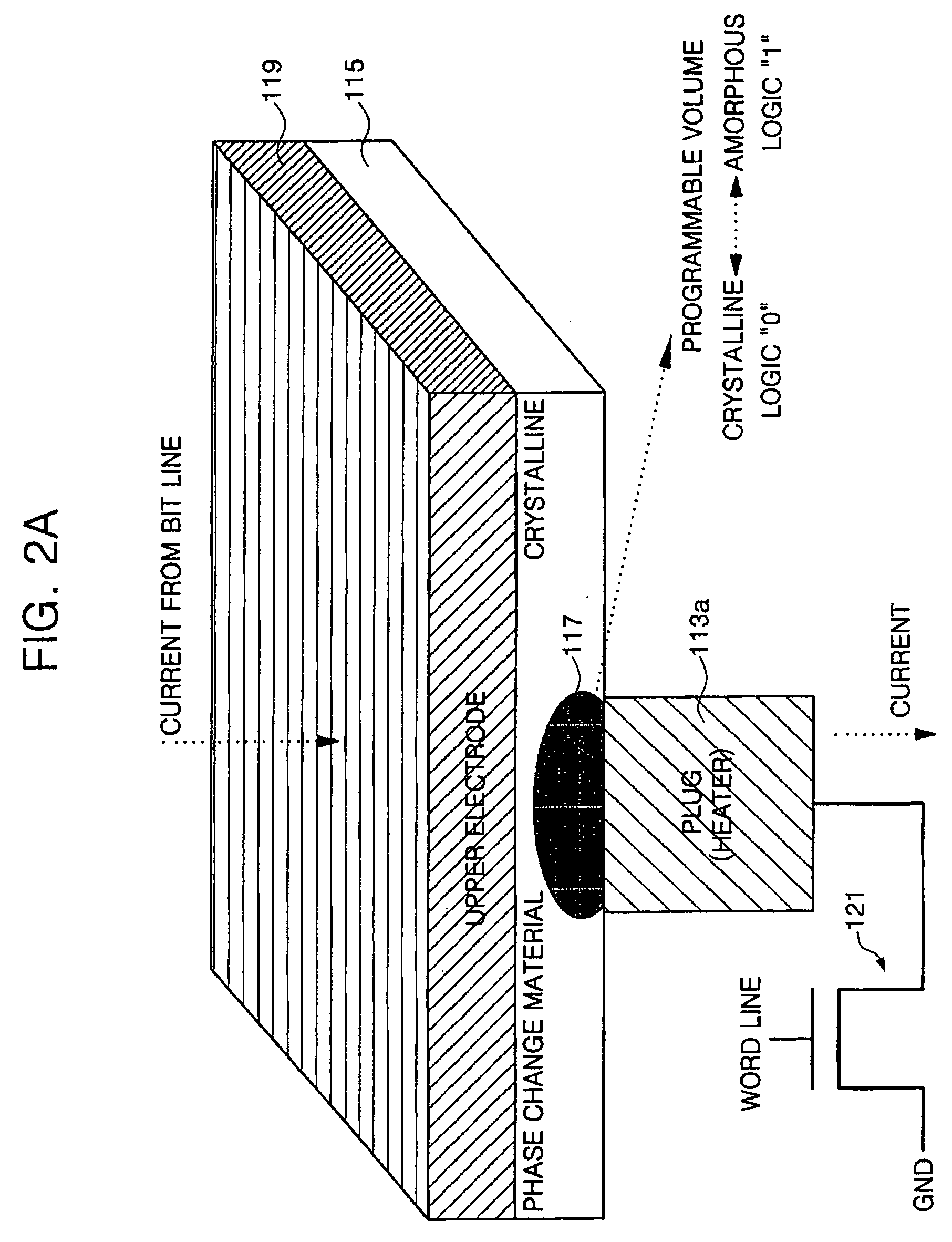
[0050]In general, the cross-sectional area of the bottom contact or heater has an effect on the programming process applied to program the programmable volume to the desired state. FIG. 3 contains a schematic cross-sectional view of a PRAM memory cell 10 illustrating a bottom contact or heater 5 in two cases in which the bottom contact or heater has one of two possible cross-sectional areas. The memory cell 10 of FIG. 3 includes a substrate 1 on ...


PUM


Abstract

A phase-change random-access memory (PRAM) device includes a chalcogenide element, the chalcogenide element comprising a material which can assume a crystalline state or an amorphous state upon application of a heating current. A first contact is connected to a first region of the chalcogenide element and has a first cross-sectional area. A second contact is connected to a second region of the chalcogenide element and having a second cross-sectional area. A first programmable volume of the chalcogenide material is defined in the first region of the chalcogenide element, a state of the first programmable volume being programmable according to a resistance associated with the first contact. A second programmable volume of the chalcogenide material is defined in the second region of the chalcogenide element, a state of the second programmable volume being programmable according to a second resistance associated with the second contact.

Description

RELATED APPLICATIONS[0001]This application relies for priority on Korean Patent Application number 10-2006-0000265, filed in the Korean Intellectual Property Office on Jan. 2, 2006, the contents of which are incorporated herein in their entirety by reference.FIELD OF THE INVENTION[0002]The invention relates to a phase-change random access memory (PRAM) and methods of fabricating and programming the same, and, more particularly, to a PRAM having contacts with controlled diameters and methods of fabricating and programming the same.BACKGROUND OF THE INVENTION[0003]Phase change memory devices have recently been developed. The phase change memory device has a nonvolatile property of maintaining stored data when its power supply is interrupted. A unit cell of the phase change memory device uses a phase change material as a data storing medium. The phase change material has two stable states, namely, an amorphous state and a crystalline state, which is controlled by heat provided to the c...

Claims


Application Information

Patent Timeline
Patent Type & Authority Applications(United States)
IPC IPC(8): H01L21/336
CPCG11C11/56G11C11/5678G11C13/0004H01L45/144H01L45/1233H01L45/126H01L45/06H10N70/8413H10N70/231H10N70/8828H10N70/826H10N70/8416
Inventor JEONG, WON-CHEOLKIM, HYEONG-JUNLEE, SE-HOPARK, JAE-HYUNJEONG, CHANG-WOOK
Owner SAMSUNG ELECTRONICS CO LTD
Why Eureka
Try Eureka