Method for Fabricating a Pillar-Shaped Phase Change Memory Element

a phase change memory element and pillar technology, applied in the field of high density memory devices, can solve the problems of not presented a solution that allows, the definition and formation of such small features, and the problem of manufacturing such devices with very small dimensions

Inactive Publication Date: 2007-07-12
MACRONIX INT CO LTD
View PDF98 Cites 214 Cited by
  • Summary
  • Abstract
  • Description
  • Claims
  • Application Information

AI Technical Summary

Problems solved by technology

Problems have arisen in manufacturing such devices with very small dimensions, and with variations in process that meets tight specifications needed for large-scale memory devices.
In particular, the need to produce memory cells with portions thereof having dimensions below 100 nm has encountered the problem that the minimum feature size...

Method used


Image

  • Method for Fabricating a Pillar-Shaped Phase Change Memory Element
  • Method for Fabricating a Pillar-Shaped Phase Change Memory Element
  • Method for Fabricating a Pillar-Shaped Phase Change Memory Element

Examples


Embodiment Construction

[0017]The following detailed description is made with reference to the figures. Preferred embodiments are described to illustrate the present invention, not to limit its scope, which is defined by the claims. Those of ordinary skill in the art will recognize a variety of equivalent variations on the description that follows.

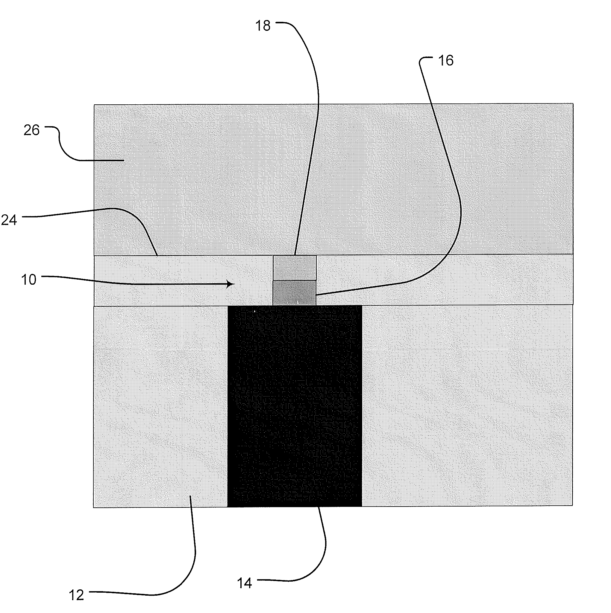
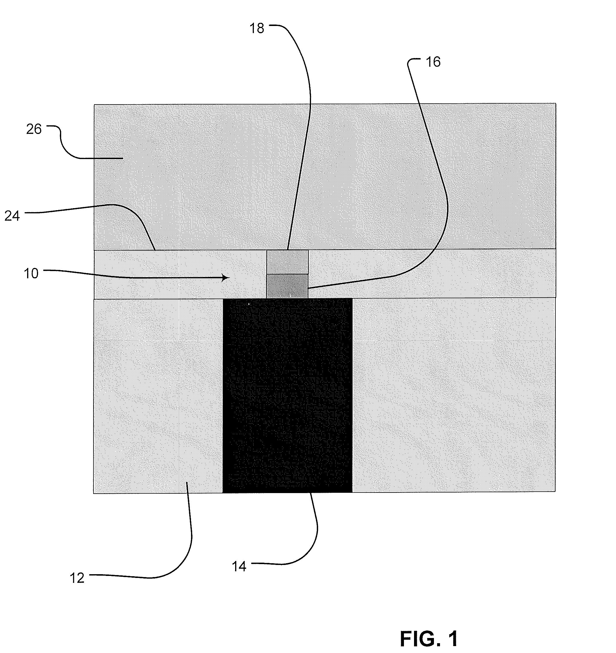
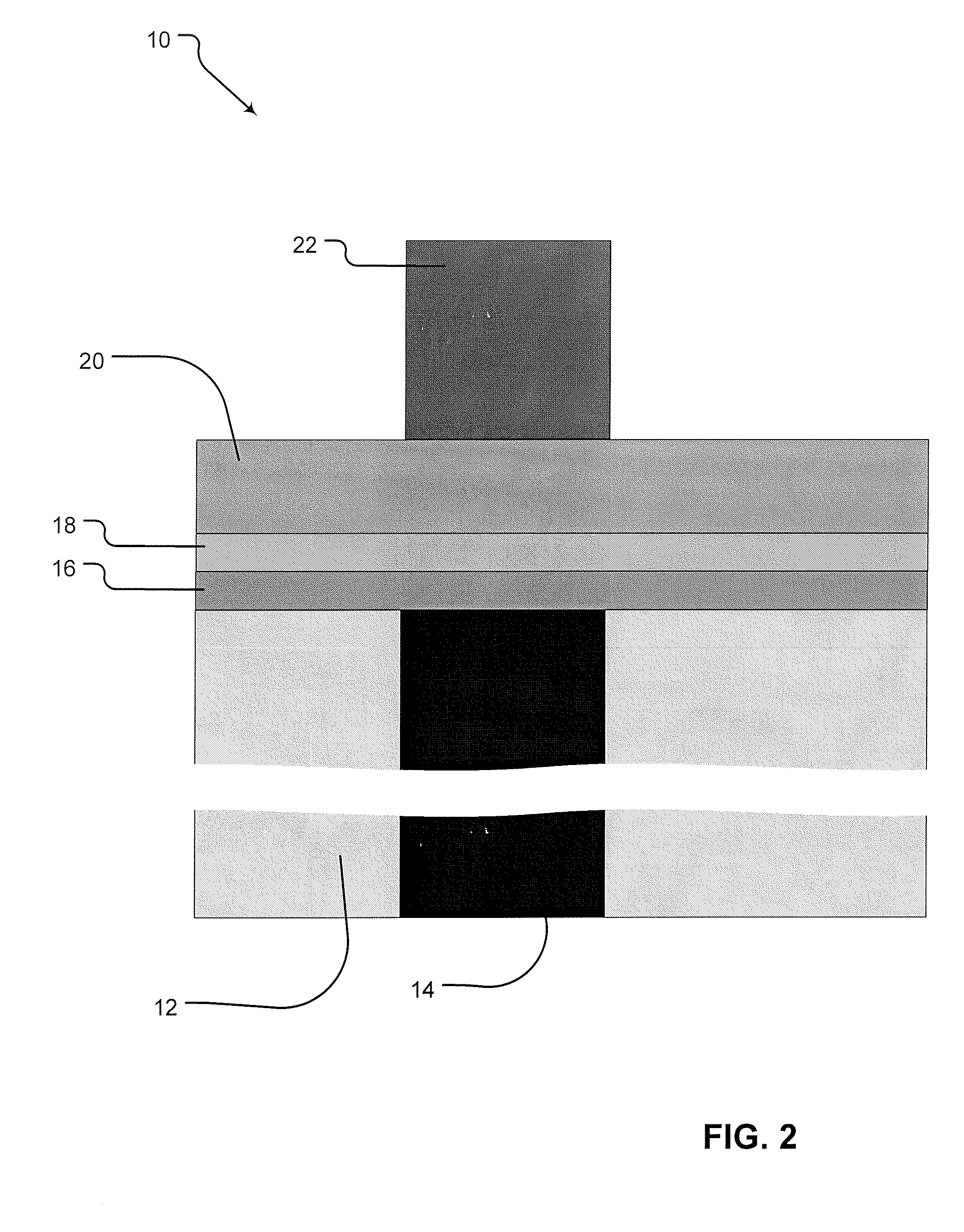
[0018]FIG. 1 depicts the pillar structure 10 of the present invention. The pillar structure is carried on a substrate 12, which typically is formed from silicon dioxide or other structure known in the art, with a contact plug 14, preferably formed from a refractory metal such as tungsten and copper, extending through the substrate to make contact with associated circuitry (not shown). Other refractory metals that could be employed include Ti, Mo, Al, Ta, Cu, Pt, Ir, La, Ni, and Ru.

[0019]The pillar itself is a relatively narrow structure having two layers—a phase change material layer 16 and an electrode layer 18. The electrode layer is a film of a material having...


PUM


Abstract

A method of fabricating a sub-feature size pillar structure on an integrated circuit. The process first provides a substrate having formed thereon a phase change layer, an electrode layer and a hard-mask layer. Then there is formed a feature-size hard-mask, by lithographically patterning, etching and stripping a photoresist layer, followed by trimming the hard-mask to a selected sub-feature size, wherein the trimming step is highly selective between the electrode and phase change material layers and the hard-mask. The final steps are trimming the electrode and phase change layers to the size of the hard-mask and removing the hard-mask.

Description

PRIORITY INFORMATION[0001]This application claims the benefit of U.S. Provisional Application No. 60 / 757,341, entitled “Method for Fabricating a Pillar-Shaped Phase Change Memory Element” filed on 9 Jan. 2006 by ChiaHua Ho.BACKGROUND OF THE INVENTION[0002]1. Field of the Invention[0003]The present invention relates to high density memory devices based on phase change based memory materials, including chalcogenide based materials and other materials, and to methods for manufacturing such devices, and most particularly to methods for fabricating such devices having dimensions smaller than the minimum feature size of a manufacturing process.[0004]2. Description of Related Art[0005]Phase change based memory materials are widely used in non-volatile random access memory cells. Such materials, such as chalcogenides and similar materials, can be caused to change phase between an amorphous state and a crystalline state by application of electrical current at levels suitable for implementati...

Claims


Application Information

Patent Timeline
IPC IPC(8): H01L47/00
CPCH01L45/06H01L45/1233H01L45/143H01L45/1691H01L45/148H01L45/1675H01L45/144H10N70/231H10N70/8825H10N70/826H10N70/884H10N70/8828H10N70/068H10N70/063
Inventor HO, CHIAHUA
Owner MACRONIX INT CO LTD
Why Eureka
Try Eureka