Programming method for flash memory capable of compensating reduction of read margin between states due to hot temperature stress

a programming method and flash memory technology, applied in the field of flash memory devices, can solve the problems of double-difficult memory system designers, increased time required to program a memory cell to a desired data state, and only exacerbated problems

Active Publication Date: 2007-07-12
SAMSUNG ELECTRONICS CO LTD
View PDF3 Cites 81 Cited by
  • Summary
  • Abstract
  • Description
  • Claims
  • Application Information

AI Technical Summary

Benefits of technology

[0016]In one embodiment, the invention provides a programming method for a flash memory device having a plurality of memory cells storing multi-bit data indicating one of a plurality of states, the programming method comprising; programming memory cells selected to have one of the plurality of states using multi-bit data, detecting programmed memory cells within a predetermined region of a threshold voltage distribution, wherein the programmed memory cells have one of the plurality of states, wherein the predetermined region is selected by one of a first verify voltage and a read voltage and a second voltage, the first verify voltage being lower than the second verify voltage and higher than the read voltage, and programming the detected memory cells to have a threshold voltage being equivalent to or higher than the second verify voltage corresponding to the respective states.
[0017]In

Problems solved by technology

Unfortunately, the ISSP and similar schemes significantly increase the time required to program a memory cell to a desired data state, particularly for small increment sizes.
Accordingly, the expansion of threshold voltage distributions due to an electric field and/or F-poly coupling effects and HTS pr

Method used


Image

  • Programming method for flash memory capable of compensating reduction of read margin between states due to hot temperature stress
  • Programming method for flash memory capable of compensating reduction of read margin between states due to hot temperature stress
  • Programming method for flash memory capable of compensating reduction of read margin between states due to hot temperature stress

Examples


Embodiment Construction

[0027]The present invention will now be described in some additional detail with reference to the accompanying drawings. This invention may, however, be embodied in many different forms and should not be construed as being limited to only the embodiments set forth herein. Rather, these embodiments are presented as teaching examples. In the drawings, like numbers refer to like or similar elements.

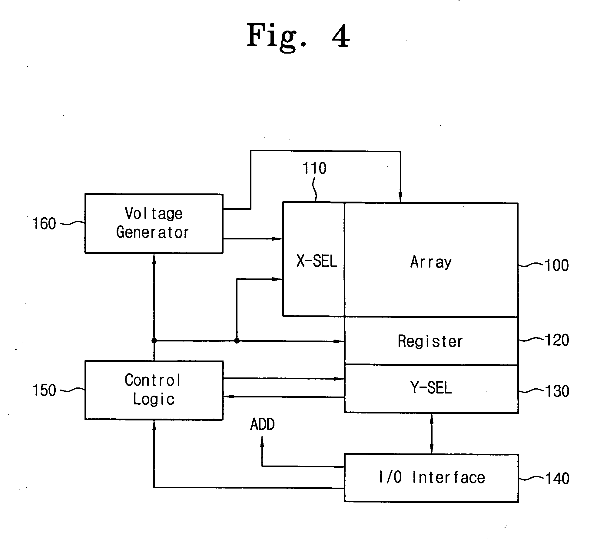
[0028]FIG. 4 is a block diagram of a flash memory device according to an embodiment of the invention. FIG. 5 is a circuit diagram further illustrating the memory cell array of FIG. 4.

[0029]Referring to FIG. 4, the illustrated flash memory device includes a memory cell array 100 adapted to store data. Memory cell array 100 includes a plurality of memory blocks each having a memory cell configuration illustrated in FIG. 5.

[0030]As illustrated in FIG. 5, a memory block MB includes a plurality of memory cell strings 101 each having a string select transistor SST, a ground select transistor GST, ...


PUM


Abstract

A program method of a flash memory device including a plurality of memory cells for storing multi-bit data indicating one of states. The program method includes programming memory cells selected to have one of the states by using multi-bit data; detecting programmed memory cells within a predetermined region of a threshold voltage distribution where the programmed memory cells having the respective states are distributed, wherein the predetermined region of the respective states is selected by one of a first verify voltage and a read voltage and a second voltage, the first verify voltage being lower than the second verify voltage and higher than the read voltage; and programming the detected memory cells to have a threshold voltage being equivalent to or higher than the second verify voltage corresponding to each of the states.

Description

BACKGROUND OF THE INVENTION[0001]1. Field of the Invention[0002]Embodiments of the invention relate to a flash memory device and, more particularly, to a programming method adapted for use with a flash memory device.[0003]This application claims priority under 35 U.S.C §119 to Korean Patent Application 2006-03584 filed on Jan. 12, 2006, the subject matter of which is hereby incorporated by reference.[0004]2. Description of the Related Art[0005]In recent years, volatile and non-volatile memory devices have been incorporated into a host of mobile appliances, such as MP3 players, cellular telephones, portable multimedia players (PMPs), notebook computers, personal digital assistances (PDAs), etc., in ever greater quantities. Emerging mobile appliances require large quantities of digital data storage to support functionality, such as motion picture playback, etc.[0006]Great effort has been expended to meet the demand for ever expanding memory in mobile appliances. One result of this eff...

Claims


Application Information

Patent Timeline
IPC IPC(8): G11C16/04G11C11/34G11C16/06
CPCG11C11/5628G11C16/0483G11C2211/5621G11C16/3454G11C16/3459G11C16/12G11C16/10G11C16/34
Inventor KANG, DONG-KULIM, YOUNG-HO
Owner SAMSUNG ELECTRONICS CO LTD
Why Eureka
Try Eureka