Method with high gapfill capability and resulting device structure

a technology of high gapfill capability and resulting device structure, which is applied in the field of integrated circuits, can solve the problems of difficult process, difficult device smallness, and inability to meet the requirements of large-scale manufacturing, and achieves effective gapfill process, improved device reliability and performance of semiconductor circuits, and convenient use

Inactive Publication Date: 2007-07-12
SEMICON MFG INT (SHANGHAI) CORP
View PDF1 Cites 6 Cited by
  • Summary
  • Abstract
  • Description
  • Claims
  • Application Information

AI Technical Summary

Benefits of technology

[0011] Many benefits are achieved by way of the present invention over conventional techniques. For example, the present technique provides an easy to use process that relies upon conventional technology. In some embodiments, an effective gapfill process is provided which improves the device reliability and performance of a semiconductor circuit. Additionally, the method provides a process that is compatible with conventional process technology without substantial modifications to conventional equipment and processes. Depending upon the embodiment, one or more of these benefits may be achieved. These and other benefits will be described in more throughout the present specification and more particularly below.

Problems solved by technology

An IC fabrication facility can cost hundreds of millions, or even billions, of dollars.
Making devices smaller is very challenging, as each process used in IC fabrication has a limit.
Additionally, as devices require faster and faster designs, process limitations exist with conventional processes and materials.
One such example of a process limitation deals with the difficulty of filling a trench that has a high aspect ratio, meaning that the ratio of the depth of the trench to the trench opening is large.
A high aspect ratio can cause problems during the trench fill process in that the deposited material is not uniformly distributed over the surface area of the trench, leading to overhang of the deposited material at the trench corner and voids at the center of the trench.
This can lead to problems with device performance and electrical reliability.

Method used


Image

  • Method with high gapfill capability and resulting device structure
  • Method with high gapfill capability and resulting device structure
  • Method with high gapfill capability and resulting device structure

Examples


Embodiment Construction

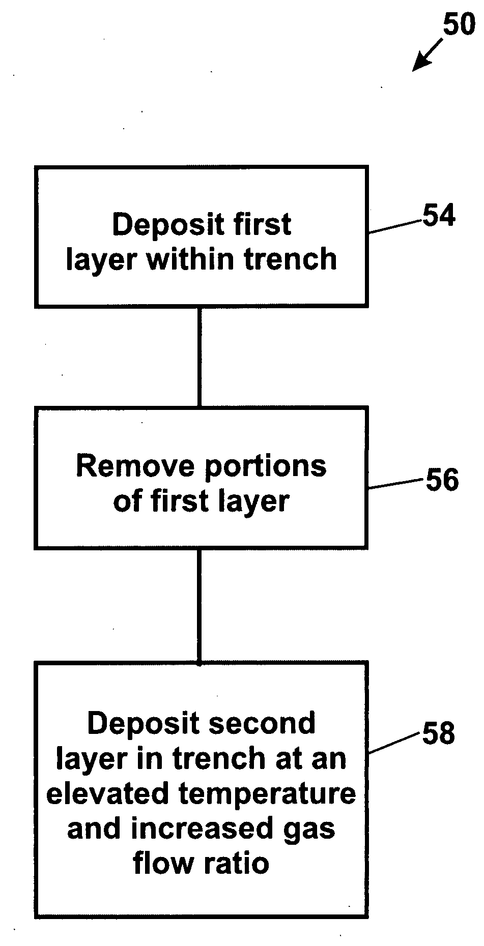
[0022] The present invention is directed to integrated circuits and their processing for the manufacture of semiconductor devices. More particularly, the invention provides an CVD deposition method with high gapfill gapfill capability and a resulting device structure. Merely by way of example, the invention has been applied to making shallow trench isolation (STI) regions. But it can be recognized that the invention has a much broader range of applicability.

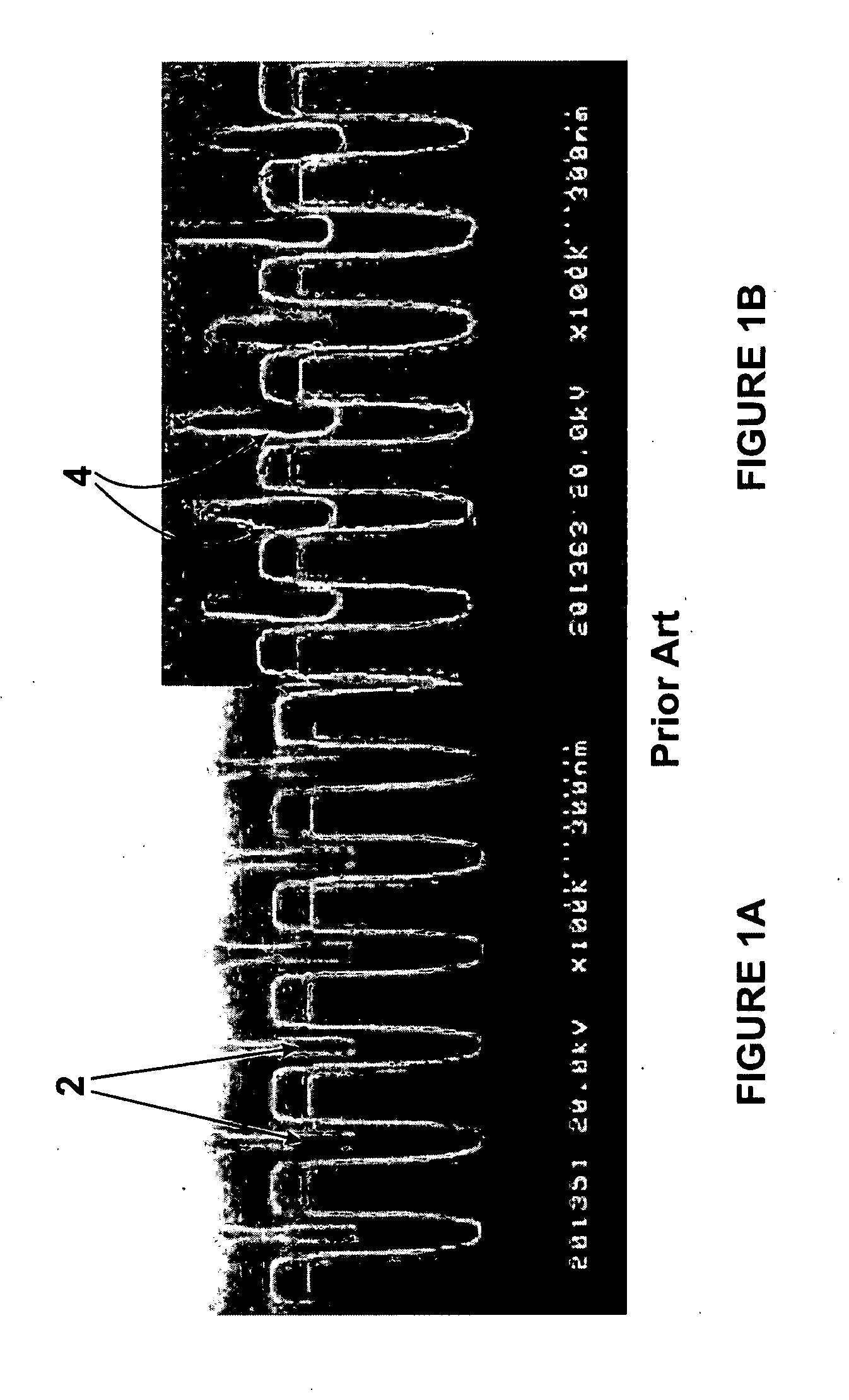
[0023]FIGS. 1A and 1B are scanning electron microscope (SEM) images of a cross-section of a silicon substrate showing voiding in a conventional trench filling process. A deposition process is used to fill the high aspect ratio trenches formed within the substrate. For example, a high aspect ratio trench is a trench where the ratio of the trench depth to the trench width is greater than 5:1. A trench with exemplary dimensions of a trench opening of 12 μm and a depth of 5000 Å can incur a number of problems when performing a depos...


PUM


Abstract

A method for filling a trench includes forming a first layer in a trench in order to partially fill the trench, removing at least a potion of the first layer from the trench; and forming a second layer on the first layer, wherein the forming a second layer is performed at a temperature of at least 700 degrees C. and at a gas flow ratio of at least 1.6, the gas flow ratio being equal to a first gas flow rate for a first gas to a second gas flow rate for a second gas. In a specific embodiment, the method includes removing a contaminant from the first layer by reacting with the contaminant present in the first layer at the temperature and with the gas flow ratio. In a specific embodiment, the removing at least a portion of the first layer includes etching the portion of the first layer.

Description

CROSS-REFERENCES TO RELATED APPLICATIONS [0001] This application claims priority to Chinese Patent Application No. 200510111129.0, filed Dec. 5, 2005, commonly assigned and of which is incorporated by reference herein for all purposes. BACKGROUND OF THE INVENTION [0002] The present invention is directed to integrated circuits and their processing for the manufacture of semiconductor devices. More particularly, the invention provides a CVD deposition method with high gapfill capability and a resulting device structure. Merely by way of example, the invention has been applied to making shallow trench isolation (STI) regions. But it can be recognized that the invention has a much broader range of applicability. [0003] Integrated circuits or “ICs” have evolved from a handful of interconnected devices fabricated on a single chip of silicon to millions of devices. Current ICs provide performance and complexity far beyond what was originally imagined. In order to achieve improvements in co...

Claims


Application Information

Patent Timeline
Patent Type & Authority Applications(United States)
IPC IPC(8): H01L21/76
CPCH01L21/02164H01L21/02271H01L21/76224H01L21/31612H01L21/02274
Inventor ANG, TING CHEONG
Owner SEMICON MFG INT (SHANGHAI) CORP
Why Eureka
Try Eureka