System and method for estimating reliability of components for testing and quality optimization

a reliability estimation and quality optimization technology, applied in the field of reliability testing and engineering, can solve problems such as defect clustering in or on base materials of nanotechnology devices, molecular computing components, nanodevices and the like, and achieve the effect of reducing scrap loss and shortening burn-in tim

Inactive Publication Date: 2007-07-12
AUBURN UNIV
View PDF34 Cites 16 Cited by
  • Summary
  • Abstract
  • Description
  • Claims
  • Application Information

AI Technical Summary

Benefits of technology

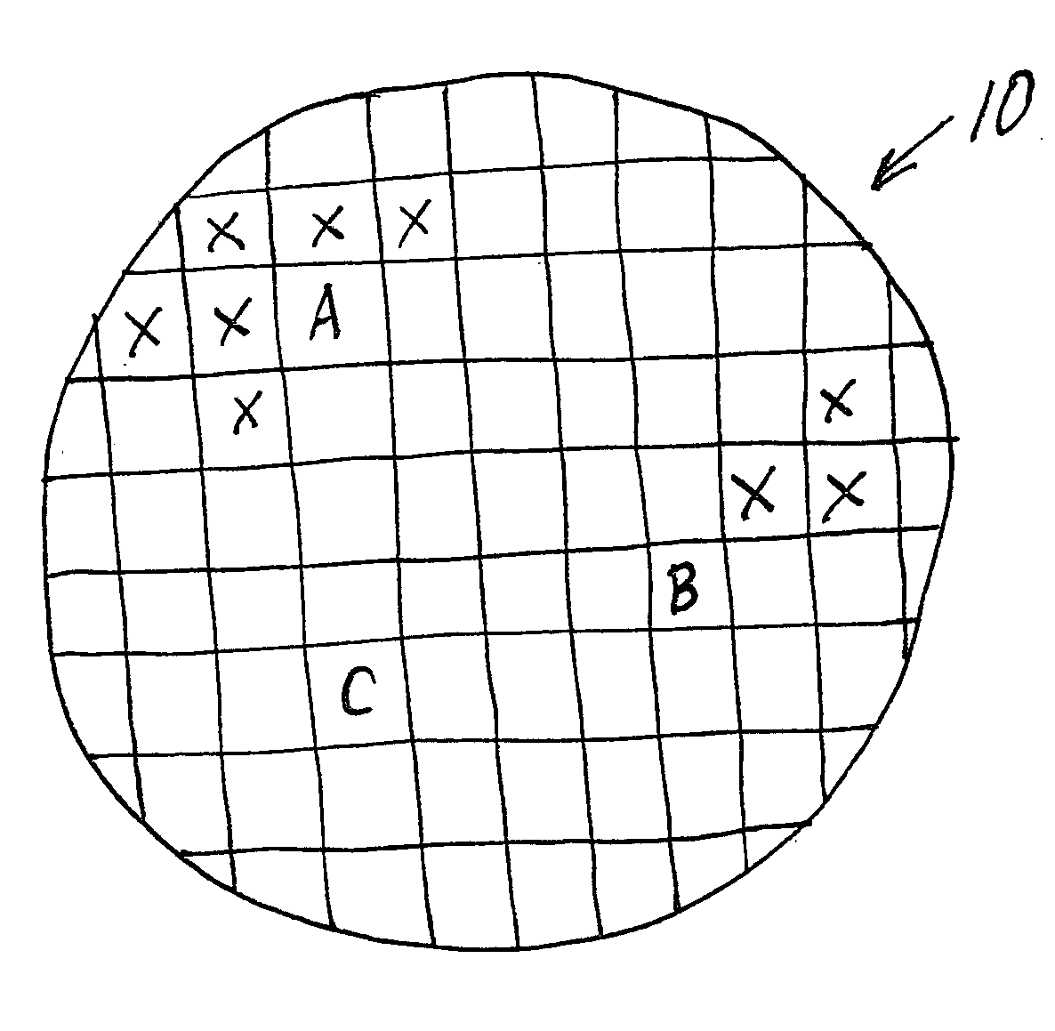
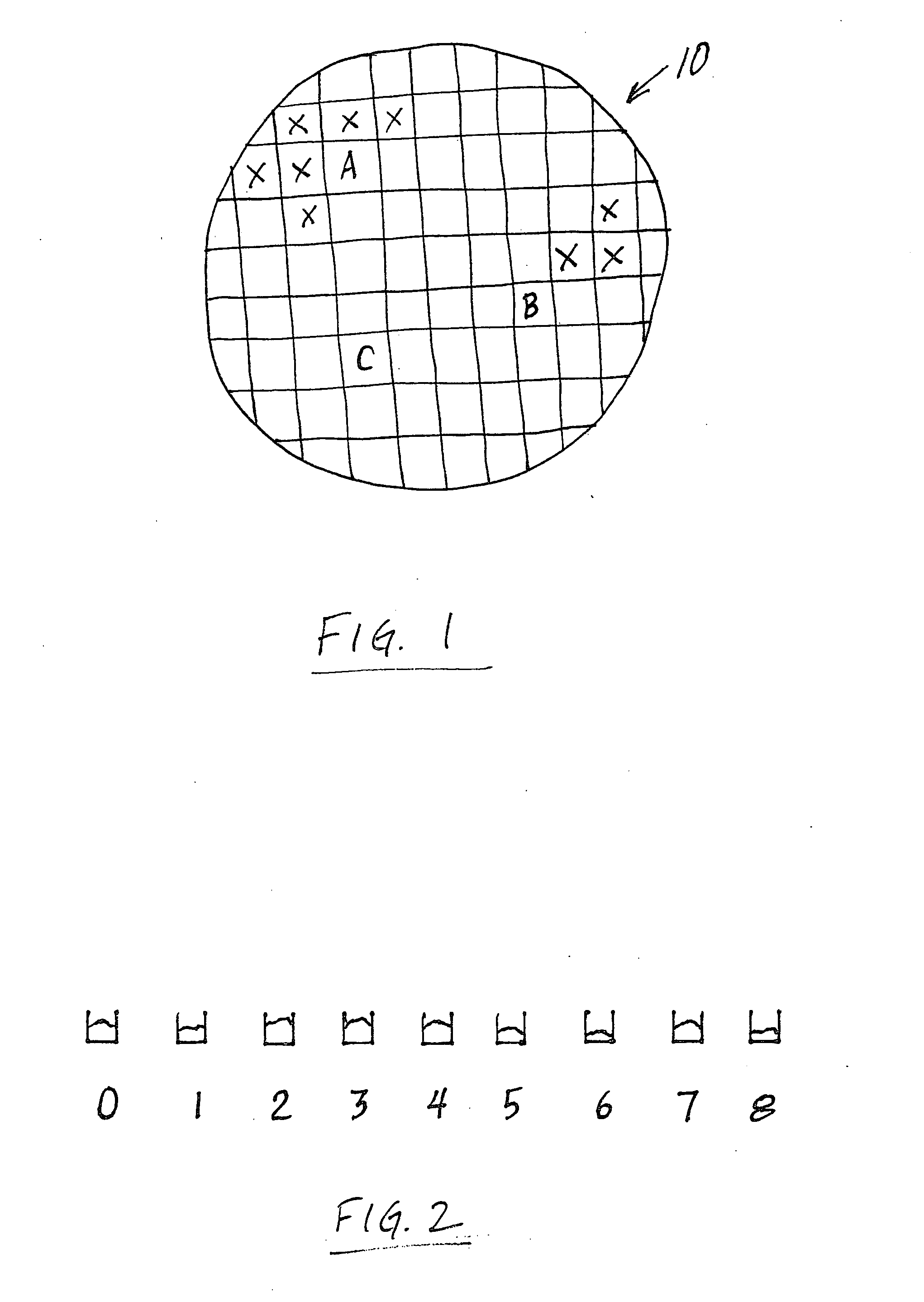
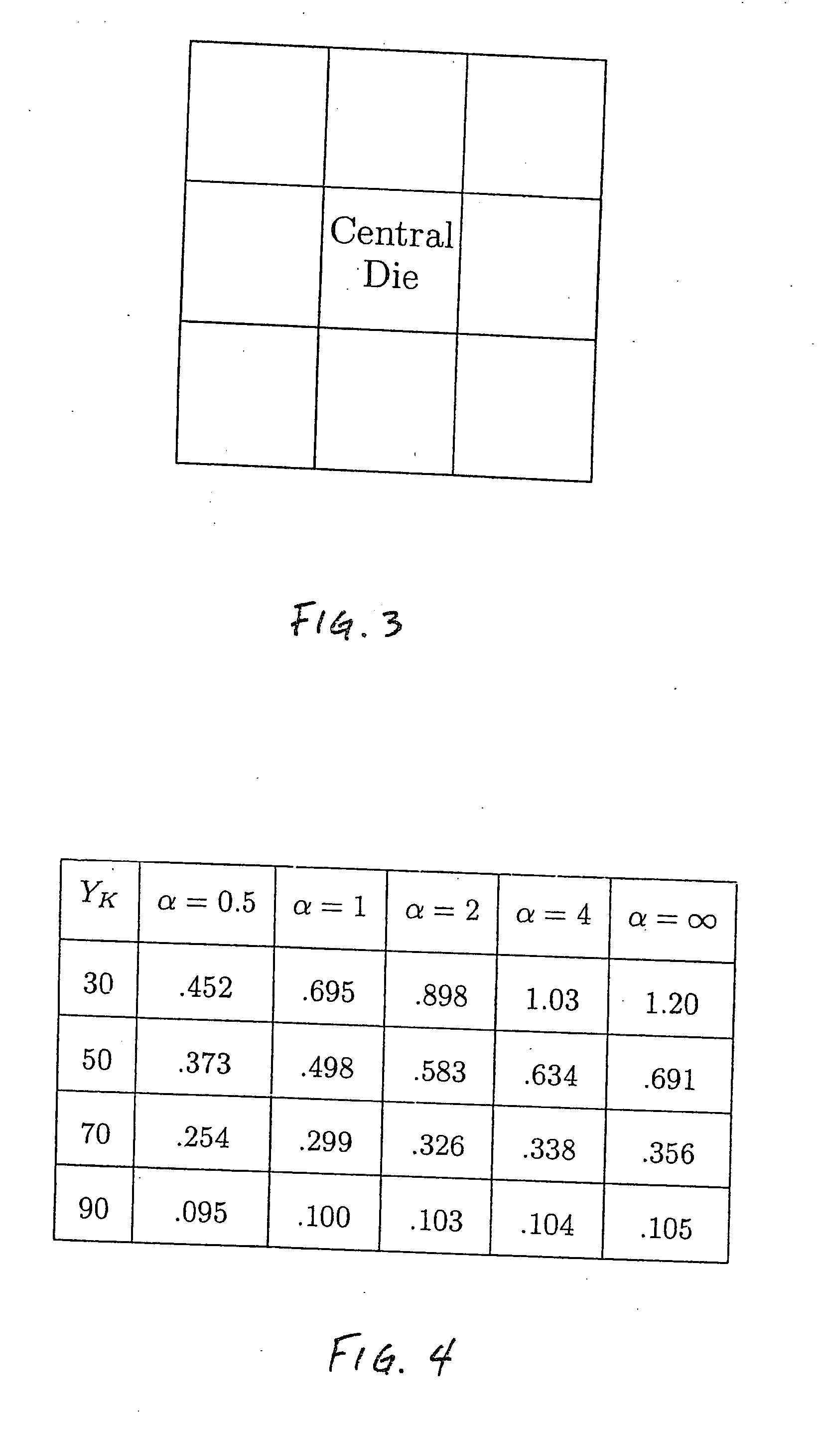
[0009] Example embodiments of the invention provide improved efficiency of reliability testing of components based on a binning and statistical modeling system. Components are binned or otherwise classified based on the number of neighboring components found to have defects by wafer probe or other form of initial testing. The number of neighboring components included in the classification scheme is not critical. As few as one neighboring component may be considered, but preferably all of the immediately neighboring components (typically numbering about 8) are considered. Neighboring components beyond the subject component's immediate neighbors optionally also can be considered, but in many instances their consideration will not add significantly to the accuracy of the model. The classification or segregation of components based on the number of defects includes classification or segregation based on the presence or absence of defects (i.e., zero defects or greater than zero defects), as well as classification or segregation based on the actual count of defects (i.e., one defect, two defects, three defects, etc.).
[0011] These reliability estimates can then be used to optimize subsequent testing, e.g. burn-in, in a number of different ways. For example, those bins determined to have a reliability rate equal to or higher than a desired or specified reliability rate need not be individually stress tested, or tested using a lower cost test such as a elevated voltage stress test instead of full burn-in. Further, if burn-in screening can ensure failure rates in the stress tested bins to be well below the specified reliability rates, then one or more bins with reliability rates somewhat below the specification can also avoid expensive burn-in as long as all the bins taken as a whole meet the overall reliability specification. Burn-in duration for the different bins can also be varied to achieve the desired reliability at minimum cost For example, components from bins with higher estimated reliability may be stress tested for a shorter duration than components from bins with lower estimated reliability. Thus, the present invention obviates the need for burn-in testing of a sample of components from each bin to determine the burn-in fallout from each bin.
[0012] In other embodiments of the invention, the reliability of a chip comprising redundant circuits that can be used to repair faulty circuitry (including, without limitation, memory chips and non-memory chips such as processor chips incorporating embedded memory) is statistically estimated, and the circuits classified for subsequent test and quality optimization, based on the number of repairs made to the subject chip itself. The need for repair, such as switching in one or more redundant rows and / or columns of memory cells in redundant memory chips, typically results from an initial test indicating the presence of a defect on the chip. Because latent defects are found to cluster with defects observed by initial testing, a chip requiring memory repairs is more likely to also have latent defects that were not observed by initial testing than a chip that did not require memory repairs. Likewise, the greater the number of memory repairs required on a chip (thereby indicating a greater number of defects observed by initial testing), the greater the likelihood of that chip also having latent defects. In other words, the more memory repairs a chip required, the less reliable that chip is.
[0015] Example embodiments of the present invention advantageously enable optimization of the duration of burn-in testing of components. For example, a shorter burn-in time can be used when testing a sample of components from the bin or classification that is statistically the most likely to have latent defects (i.e., the bin of components having the most neighbors with killer defects or the bin of components that required the greatest number of redundant memory repairs) than would be needed for testing components from the other bins or classifications, as a statistically significant number of failures due to latent defects will generally take less time to precipitate from such a sample.
[0016] The system and method of the present invention are also well suited to reliability screening of die for use in multi-chip modules (MCMs) or other composite electronic devices assembled from components that cannot be stress tested. Because burn-in testing of bare die for MCMs is difficult and expensive, MCMs are typically burned in after assembly of the dies into an MCM. A single failing die generally results in scrapping of the entire high-cost MCM. Using only die from the bin or classification that is statistically the least likely to have latent defects (i.e., the bin of components having the least neighbors with killer defects or the bin of components that required the fewest number of redundant memory repairs) can significantly reduce scrap loss.

Problems solved by technology

For example, nanotechnology devices such as molecular computing components, nanodevices and the like, may exhibit defect clustering in or on the base materials from which they are produced.

Method used


Image

  • System and method for estimating reliability of components for testing and quality optimization
  • System and method for estimating reliability of components for testing and quality optimization
  • System and method for estimating reliability of components for testing and quality optimization

Examples


Embodiment Construction

[0037] The present invention may be understood more readily by reference to the following detailed description of the invention taken in connection with the accompanying drawing figures, which form a part of this disclosure. It is to be understood that this invention is not limited to the specific devices, methods, conditions or parameters described and / or shown herein, and that the terminology used herein is for the purpose of describing particular embodiments by way of example only and is not intended to be limiting of the claimed invention. Also, as used in the specification including the appended claims, the singular forms “a,”“an,” and “the” include the plural, and reference to a particular numerical value includes at least that particular value, unless the context clearly dictates otherwise. Ranges may be expressed herein as from “about” or “approximately” one particular value and / or to “about” or “approximately” another particular value. When such a range is expressed, anothe...


PUM


Abstract

A system and method for determining the early life reliability of an electronic component, including classifying the electronic component based on an initial determination of a number of fatal defects, and estimating a probability of latent defects present in the electronic component based on that classification with the aim of optimizing test costs and product quality.

Description

CROSS-REFERENCE TO RELATED APPLICATIONS [0001] This application claims the benefit of U.S. Provisional Patent Application Ser. No. 60 / 347,974, filed Oct. 19, 2001; U.S. Provisional Patent Application Ser. No. 60 / 335,108, filed Oct. 23, 2001; and U.S. Provisional Patent Application Ser. No. 60 / 366,109, filed Mar. 20, 2002; all of which are hereby incorporated herein by reference in their entireties for all purposes.FIELD OF THE INVENTION [0002] The present invention relates generally to the field of reliability testing and engineering; and more particularly to a yield-reliability model based system and method for classifying electronic components and other devices including integrated circuits and memory chips based on predicted early life reliability to allow optimization of test costs and product quality. BACKGROUND OF THE INVENTION [0003] Electronic components such as integrated circuits, including memory chips, often fail due to flaws resulting from the manufacturing process. Ind...

Claims


Application Information

Patent Timeline
Patent Type & Authority Applications(United States)
IPC IPC(8): G06F19/00G01R31/28H01L21/66
CPCH01L22/20G01R31/287
Inventor SINGH, ADIT D.BARNETT, THOMAS S.
Owner AUBURN UNIV
Why Eureka
Try Eureka