Thin film transistor, its manufacture method and display device
a thin film transistor and manufacturing method technology, applied in non-linear optics, instruments, optics, etc., can solve the problems of inability to use transistors with leak current larger than a certain amount in practice, poor operation performance of polycrystals with a small diameter, and difficulty in forming polycrystals with an average crystal grain diameter of 1 m or larger, etc., to achieve easy manufacturing of elements, high speed operation, and small leak current
- Summary
- Abstract
- Description
- Claims
- Application Information
AI Technical Summary
Benefits of technology
Problems solved by technology
Method used
Image
Examples
first embodiment
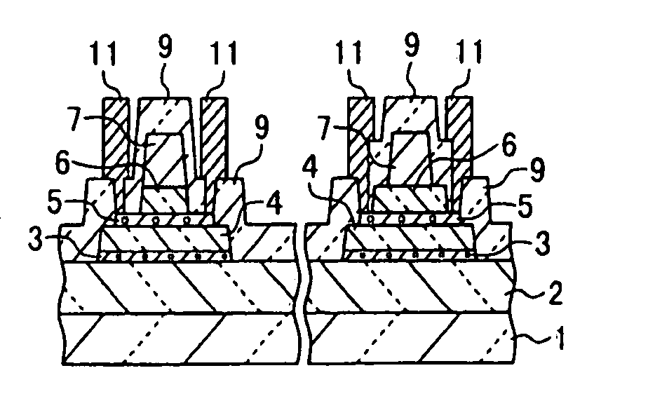
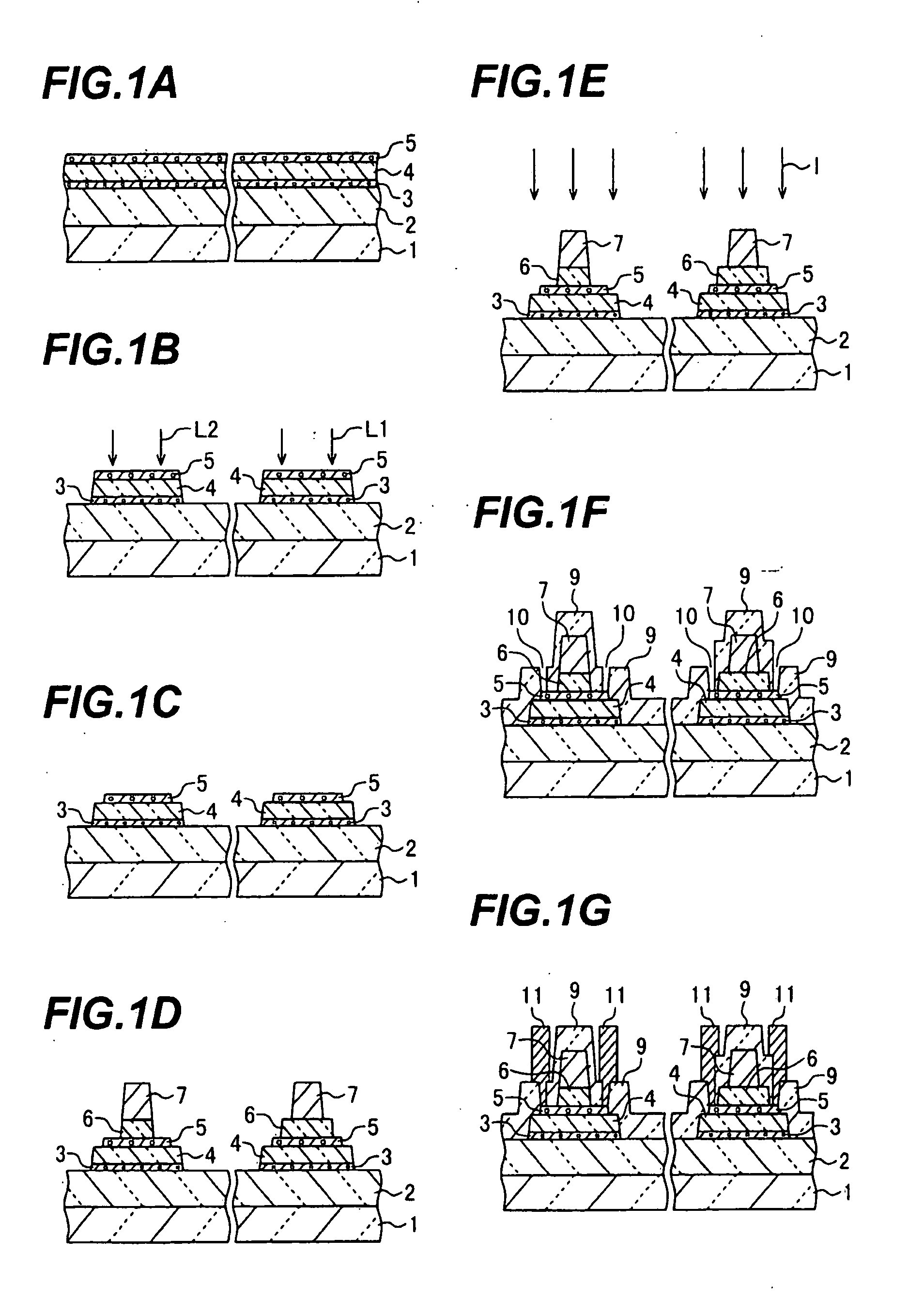
[0027]FIGS. 1A to 1G are schematic cross sectional views illustrating a thin film transistor manufacture method according to the invention. Referring first to FIG. 1A, formed on an insulating substrate 1 made of, e.g., glass having a heat resistance temperature of 650° C. are a first buffer layer 2, a heat accumulating-light shielding layer 3, a second buffer layer 4 and a semiconductor layer 5 stacked in this order from the bottom by chemical vapor deposition (CVD). For example, the first buffer layer 2 is made of silicon oxide (SiO) and has a thickness of 400 nm, the heat accumulating-light shielding layer 3 is made of amorphous silicon and has a thickness of 50 nm, the second buffer layer 4 is made of silicon oxide and has a thickness of 100 nm, and the semiconductor layer 5 is made of amorphous silicon and has a thickness of 75 nm.
[0028] Referring to FIG. 1B, the heat accumulating-light shielding layer 3, second buffer layer 4 and semiconductor layer 5 are worked by photolithogr...
second embodiment
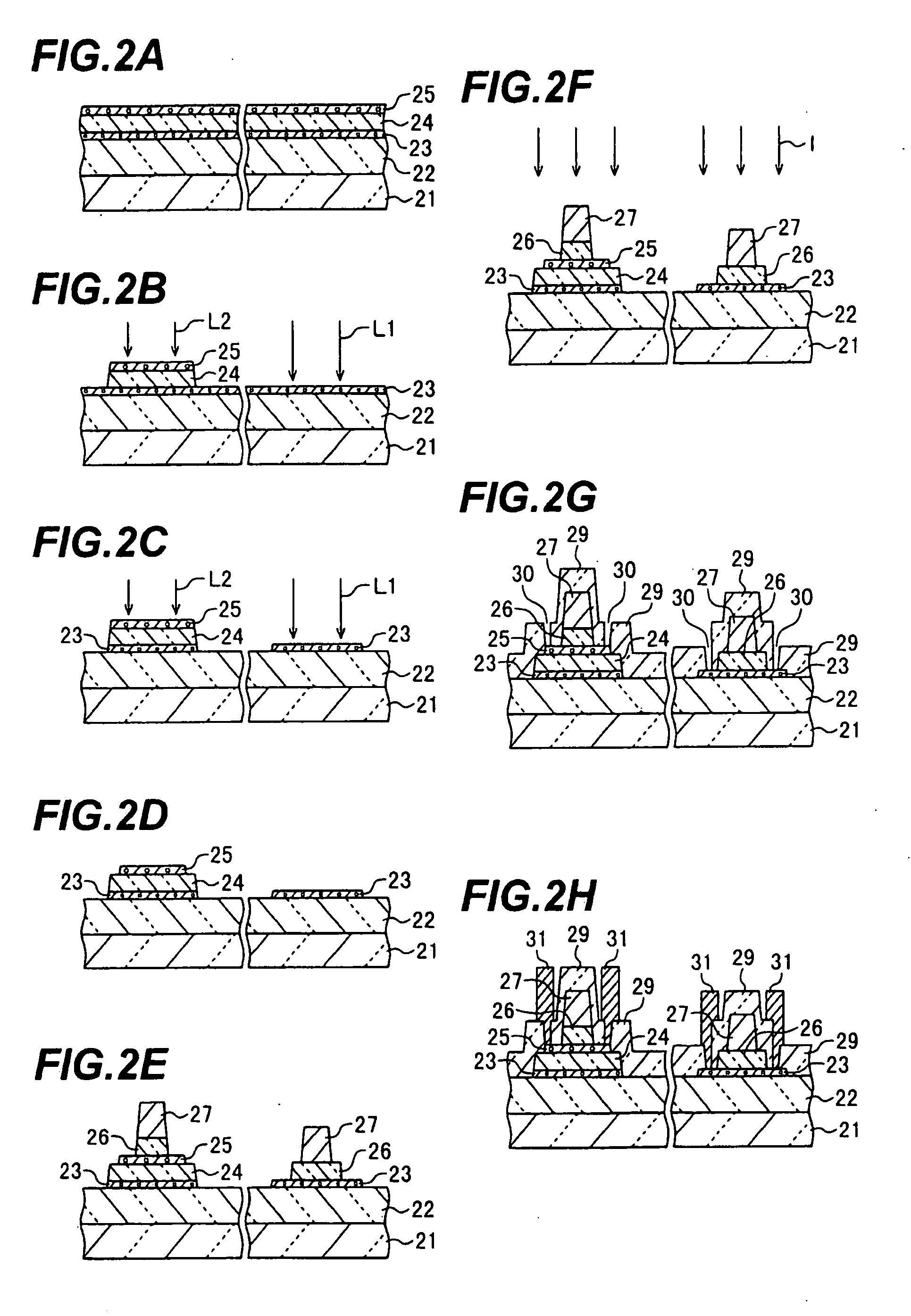
[0062] The structures of the transistors manufactured by the second embodiment method are not limited only to those described above. For example, Offset or LDD regions may be formed in partial regions of the second semiconductor layer 25 of the transistor in the left area.
[0063] A continuously oscillating laser beam may be used to crystallize the first semiconductor layer 23 in the right area, similar to crystallizing the second semiconductor layer 25 in the left area. In this case, for example, a second order harmonics wave (wavelength: 532 nm) of a continuously oscillating Nd:YVO4 laser beam is applied at a power of 6 W. A laser beam having an elongated beam spot shape of, e.g., a length of 400 μm and a width of 40 μm is applied while it is scanned along a beam spot width direction at a speed of about 400 mm / sec for example. Since the thickness of the first semiconductor layer 23 is only 50 nm, the silicon crystals are not changed to have a large crystal grain diameter, but the cr...
PUM
| Property | Measurement | Unit |
|---|---|---|
| average crystal grain diameter | aaaaa | aaaaa |
| thickness | aaaaa | aaaaa |
| thickness | aaaaa | aaaaa |
Abstract
Description
Claims
Application Information


