Integrated MIS photosensitive device using continuous films

a photosensitive device and continuous film technology, applied in the field of image sensors, can solve the problems of low signal level of mesa-isolated mis and p-i-n photodiode sensors, disadvantages of conventional photosensitive devices, and poor image signals of isolating mis and p-i-n photodiodes

Inactive Publication Date: 2007-07-19
VAREX IMAGING CORP
View PDF17 Cites 25 Cited by
  • Summary
  • Abstract
  • Description
  • Claims
  • Application Information

AI Technical Summary

Benefits of technology

[0014] In accordance with another embodiment of the presently claimed invention, an integrated photosensitive device includes a substrate and an MIS photodiode at least a portion of which is disposed over the substrate. The MIS photodiode includes: a plurality of conduction layers including at least first, second and third conduction layers comprising first, second and third films of conductive material, respectively; one or more insulation layers at least a portion of at least one of which is disposed between the first and second conduction layers, wherein at least one of the one or more insulation layer portions comprises a respective substantially continuous film of insulation material; and one or more semiconductor layers at least a portion of at least one of which is disposed between one of the one or more insulation layers and one of the first and second conduction layers, wherein at least one of the one or more semiconductor layer portions comprises a respective substantially continuous film of semiconductor material; wherein one of the first and second conduction layers includes a perimeter, and said third conduction layer is disposed, at least in part, in a non-coplanar manner along part of the perimeter.
[0015] In accordance with another embodiment of the presently claimed invention, an integrated photosensitive array includes a substrate and a plurality of MIS photodiodes at least a portion of which is disposed in an array over the substrate. Each one of the at least a portion of the plurality of MIS photodiodes includes: first and second electrodes; one or more dielectrics at least a portion of at least one of which is disposed between the first and second electrodes, wherein at least one of the one or more dielectric portions comprises a respective substantially continuous layer of dielectric material; one or more semiconductors at least a portion of at least one of which is disposed between one of the one or more dielectrics and one of the first and second electrodes, wherein at least one of the one or more semiconductor portions comprises a respective substantially continuous layer of semiconductor material; and a third electrode a portion of which is disposed, at least in part, in a non-coplanar manner along a peripheral portion of one of said first and second electrodes.
[0016] In accordance with another embodiment of the presently claimed invention, an integrated photosensitive device includes a substrate and an MIS photodiode at least a portion of which is disposed over the substrate. The MIS photodiode includes: first and second electrodes; one or more dielectrics at least a portion of at least one of which is disposed between the first and second electrodes, wherein at least one of the one or more dielectric portions comprises a respective substantially continuous layer of dielectric material; one or more semiconductors at least a portion of at least one of which is disposed betw

Problems solved by technology

However, such conventional photosensitive devices have disadvantages.
Both the mesa-isolated MIS and p-i-n photodiodes typically generate poor image signals.
As noted above, a disadvantage common to mesa-isolated MIS and p-i-n photodiode sensors is l

Method used


Image

  • Integrated MIS photosensitive device using continuous films
  • Integrated MIS photosensitive device using continuous films
  • Integrated MIS photosensitive device using continuous films

Examples


Embodiment Construction

[0037] The following detailed description is of example embodiments of the presently claimed invention with references to the accompanying drawings. Such description is intended to be illustrative and not limiting with respect to the scope of the present invention. Such embodiments are described in sufficient detail to enable one of ordinary skill in the art to practice the subject invention, and it will be understood that other embodiments may be practiced with some variations without departing from the spirit or scope of the subject invention.

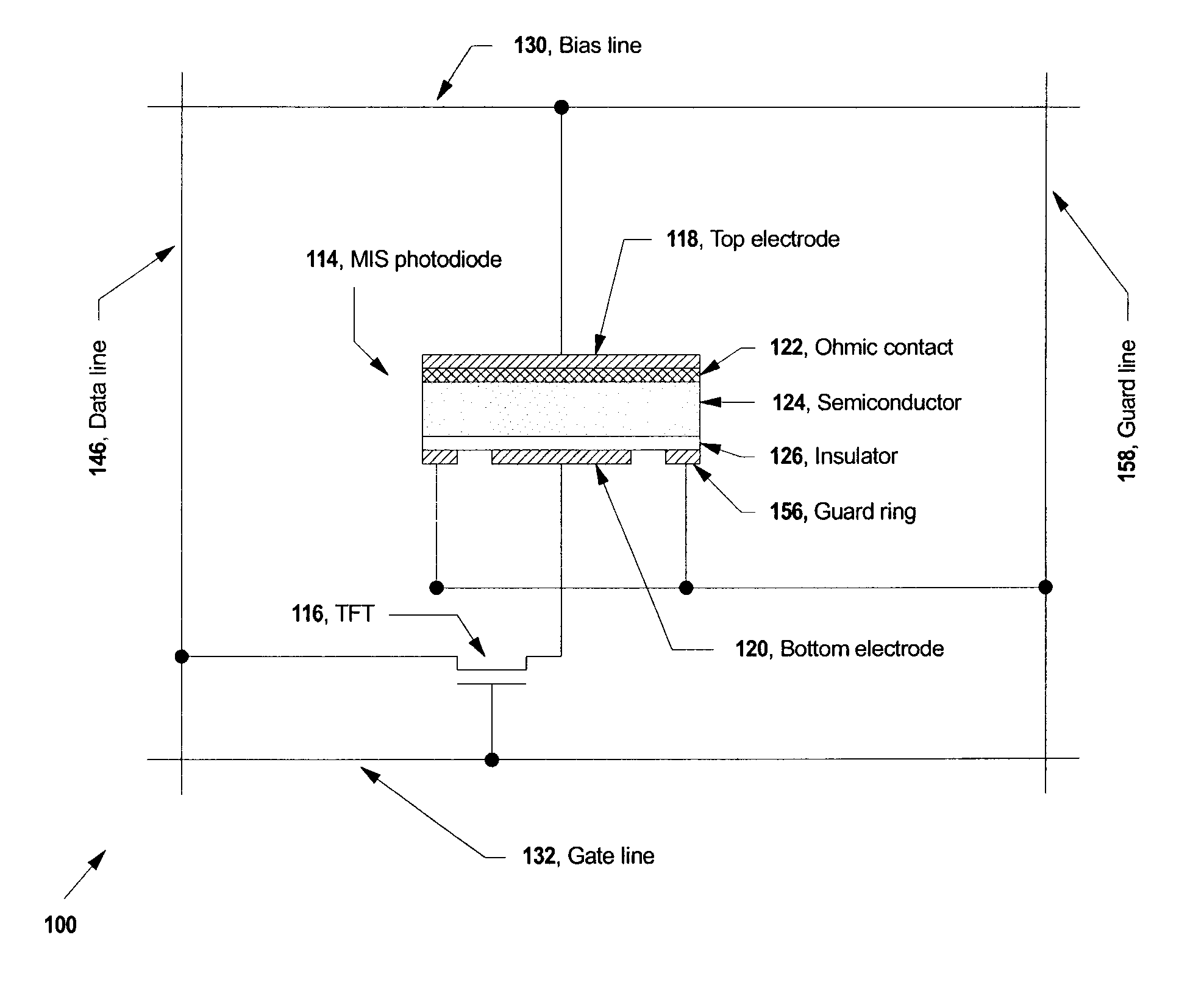
[0038] Referring to FIG. 4, a pixel circuit 100 in accordance with one embodiment of the presently claimed invention includes the MIS photodiode 114 and a TFT 116 connected to a bias line 130, gate line 132 and data line 146, all in accordance with well known pixel circuit techniques. The MIS photodiode 114 includes an optically transparent top electrode 118 and a bottom electrode 120, between which are the semiconductor layers 122, 124 and ...


PUM


Abstract

An integrated photosensitive device with a metal-insulator-semiconductor (MIS) photodiode constructed with one or more substantially continuous layers of semiconductor material and with a substantially continuous layer of dielectric material.

Description

RELATED APPLICATIONS [0001] This is continuation-in-part of U.S. patent application Ser. No. 10 / 882,603, filed Jul. 1, 2004, and entitled “Integrated MIS Photosensitive Device Using Continuous Films”.BACKGROUND OF THE INVENTION [0002] 1. Field of the Invention [0003] The present invention relates to image sensors, and in particular, to image sensors with pixel circuits implemented with metal-insulator-semiconductor (MIS) photodiodes. [0004] 2. Description of the Related Art [0005] Image sensors, such as those used for large area X-ray imaging, often use pixel circuits in which a mesa-isolated MIS photodiode is used as the photosensitive device. (A mesa-isolated device is formed by etching away a portion of the active materials, leaving a “mesa” of active materials.) Another common photosensitive device is a mesa-isolated p-i-n photodiode. Yet another conventional photosensitive device is a p-i-n photodiode comprised substantially of continuous films. However, such conventional photo...

Claims


Application Information

Patent Timeline
IPC IPC(8): H01L31/113
CPCH01L27/12H01L31/1133H01L27/14665H01L27/1463H01L31/113H01L31/12
Inventor WRIGHT, MICHAEL DEAN
Owner VAREX IMAGING CORP
Why Eureka
Try Eureka