

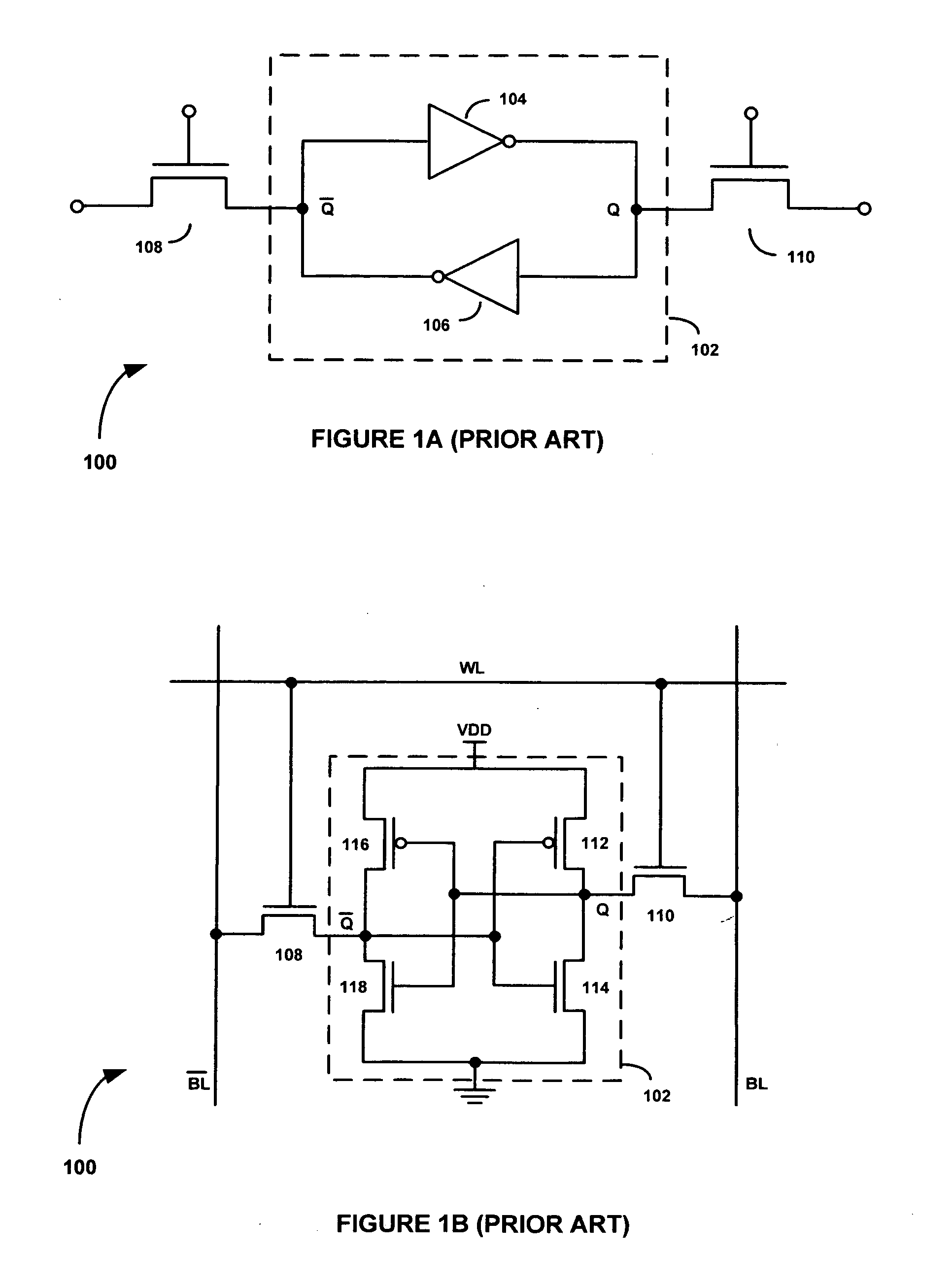
SEU hardened latches and memory cells using progrmmable resistance devices
a technology of progrmmable resistance and latches, which is applied in the field of electromechanical latches and memory cells, can solve the problems of affecting the performance of the memory cell, the dram technology is not well suited to high-capacity, low-cost applications such as personal computer (pc) memory, and the sensing of the dram cell, for example to refresh the cell, can be problematic, and be susceptible to radiation-induced soft errors. , to achieve the effect o
- Summary
- Abstract
- Description
- Claims
- Application Information
AI Technical Summary
Benefits of technology
Problems solved by technology
Method used
Image

Examples
Embodiment Construction
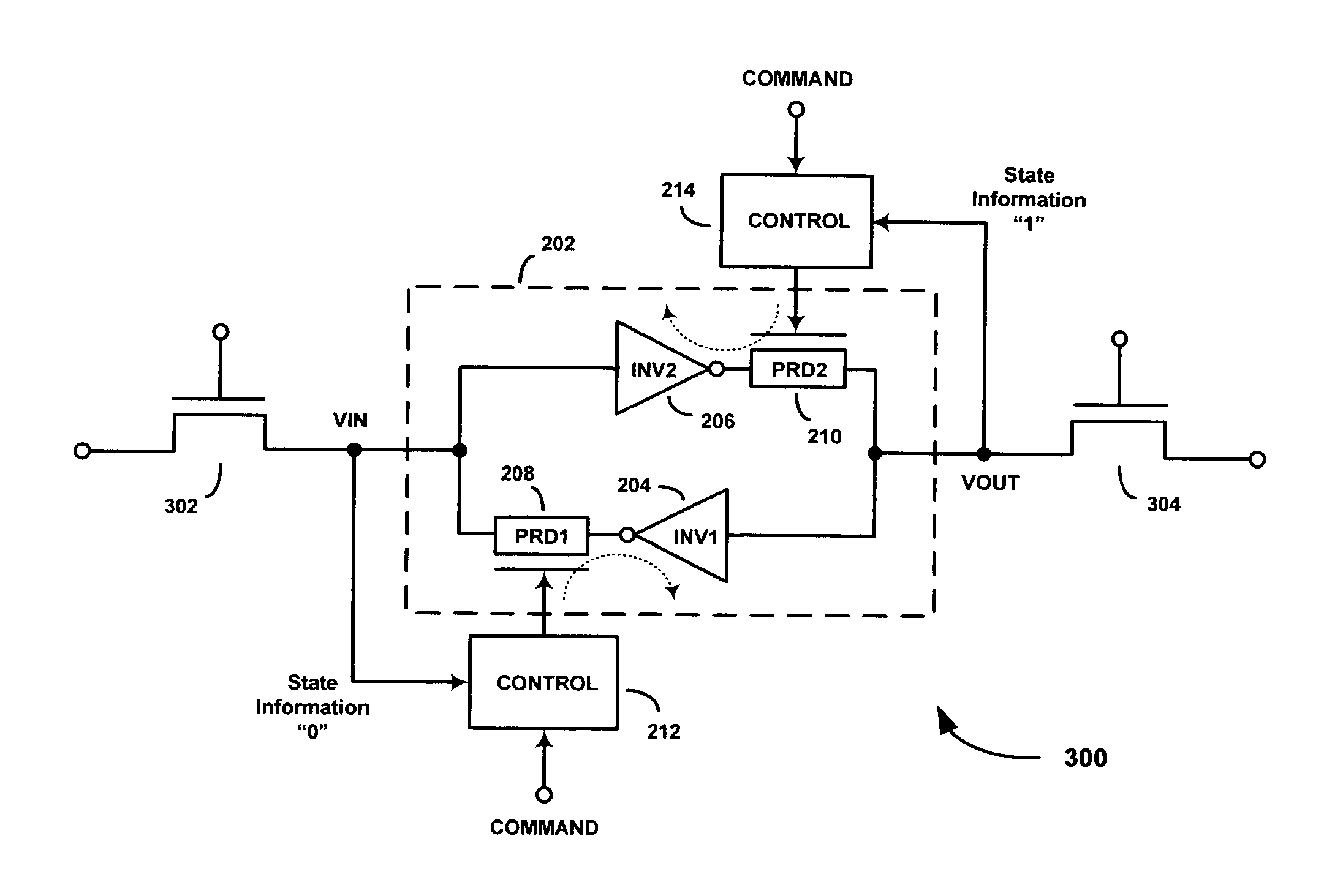
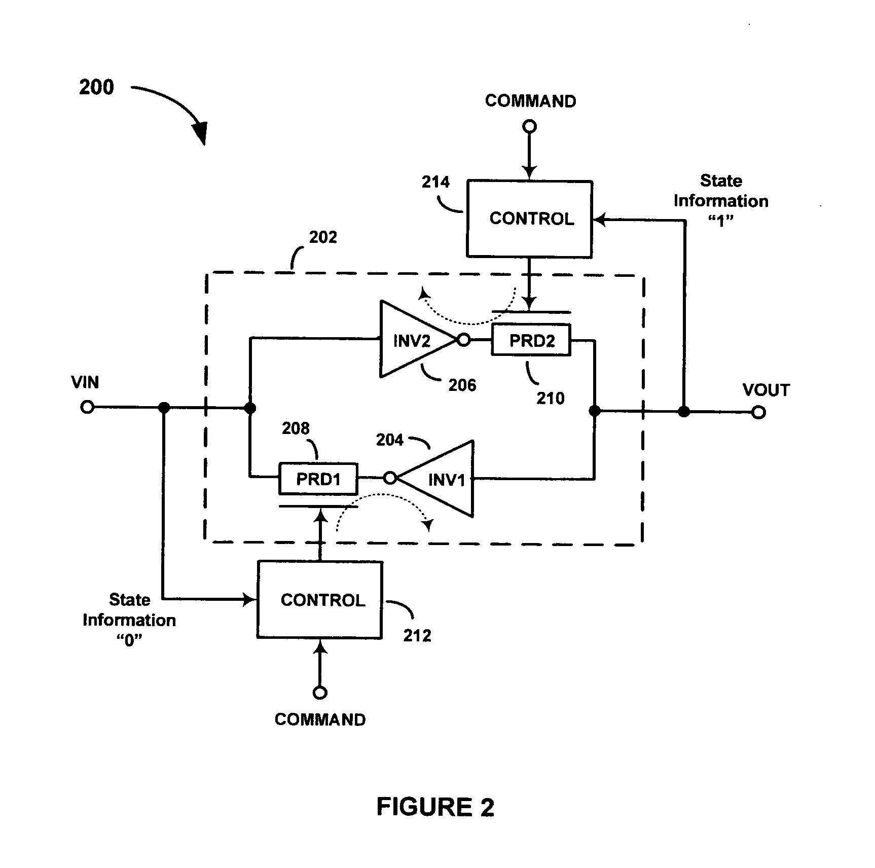
[0030] Referring to FIG. 2, there is shown an SEU hardened latch circuit 200, according to an embodiment of the present invention. The SEU hardened latch circuit 200 comprises an SEU hardened latch 202 that includes first and second inverters 204 and 206 (INV1 and INV2) and first and second programmable resistance devices 208 and 210 (PRD1 and PRD2). The first inverter (INV2) 204 has an input that is coupled to a latch output terminal VOUT and an output that is coupled to a first terminal of the first PRD (PRD1) 208. A second terminal of the first PRD (PRD1) 208 is coupled to a latch input terminal VIN. A third terminal of the first PRD (PRD1) 208 is coupled to a control output of a first control module 212, which includes a state information input that is coupled to the latch input terminal VIN. The second inverter (INV2) 206 has an input that is coupled to the latch input terminal VIN and an output that is coupled to a first terminal of the second PRD (PRD2) 210. A second terminal...
PUM
 Abstract
Description
Claims
Application Information