Semiconductor constructions, methods of forming semiconductor constructions, light-conducting conduits, and optical signal propagation assemblies

a technology of semiconductor construction and semiconductor structure, which is applied in the direction of instruments, cladded optical fibres, optical elements, etc., can solve the problem of rendering electrons incapable of being utilized for transferring information at ultra-fast processor speeds

Active Publication Date: 2007-07-19
MICRON TECH INC
View PDF4 Cites 5 Cited by
  • Summary
  • Abstract
  • Description
  • Claims
  • Application Information

AI Technical Summary

Benefits of technology

[0006] In one aspect, the invention includes a light-directing conduit. The conduit includes an inner material through which light migrates, and a sheath (or barrier) around the inner material. The sheath is configured to substantially keep the light migrating along a path defined by the inner material. The inner material comprises a matrix having one or more rare earth elements dispersed therein, with a total concentration of the one or more rare earth elements within at least a portion of the matrix being at least about 1×10¹⁶ atoms / cm3. As is known to persons of ordinary skill in the art, rare earth elements are any of the elements having atomic numbers 58-71.
[0007] In one aspect, the invention includes a semiconductor construction comprising a semiconductor substrate, and a waveguide supported by the substrate. The waveguide comprises one or more rare earth elements, with such elements being present to a total concentration of at least about 1×10¹⁶ atoms / cm3 within at least one segment of the waveguide.
[0008] In one aspect, the invention includes an optical signal propagation assembly. The assembly comprises an optical signal input, an optical signal amplifier, an optical signal receiver, and an optical signal conduit. The optical signal amplifier is configured to receive an optical signal from the input and amplify the optical signal, and the optical signal conduit is configured to direct the amplified signal from the amplifier to the receiver. The optical signal amplifier comprises one or more rare earth elements within a matrix material. In particular aspects, the rare earth elements can include one or more of cerium, erbium, neodymium and ytterbium.
[0009] In one aspect, the invention includes a method of forming a semiconductor construction. A semiconductor substrate provided, and one or more trenches are etched into the substrate. At least one of the trenches is lined with a first barrier material, and then filled with a waveguide material. At least some of the waveguide material is doped with one or more rare earth elements. A second barrier material is then formed over the waveguide material, with the second barrier material contacting the first barrier material along sidewalls of the at least one trench.

Problems solved by technology

At very high frequencies, numerous physical effects degrade performance of electrons as dependable carriers of information, rendering the electrons incapable of being utilized for transferring information at ultra-fast processor speeds.

Method used


Image

  • Semiconductor constructions, methods of forming semiconductor constructions, light-conducting conduits, and optical signal propagation assemblies
  • Semiconductor constructions, methods of forming semiconductor constructions, light-conducting conduits, and optical signal propagation assemblies
  • Semiconductor constructions, methods of forming semiconductor constructions, light-conducting conduits, and optical signal propagation assemblies

Examples


Embodiment Construction

[0021] This disclosure of the invention is submitted in furtherance of the constitutional purposes of the U.S. Patent Laws “to promote the progress of science and useful arts” (Article 1, Section 8).

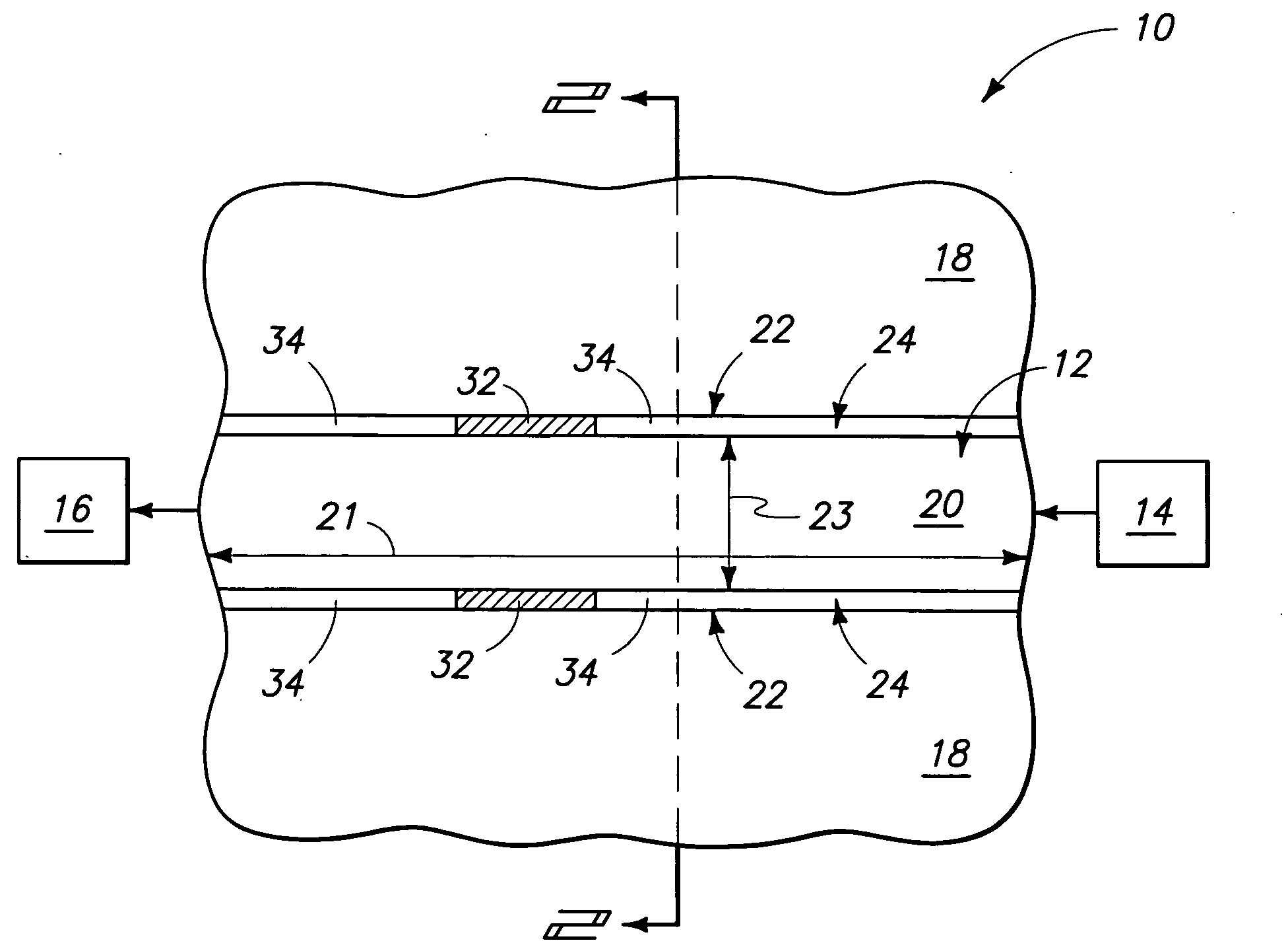
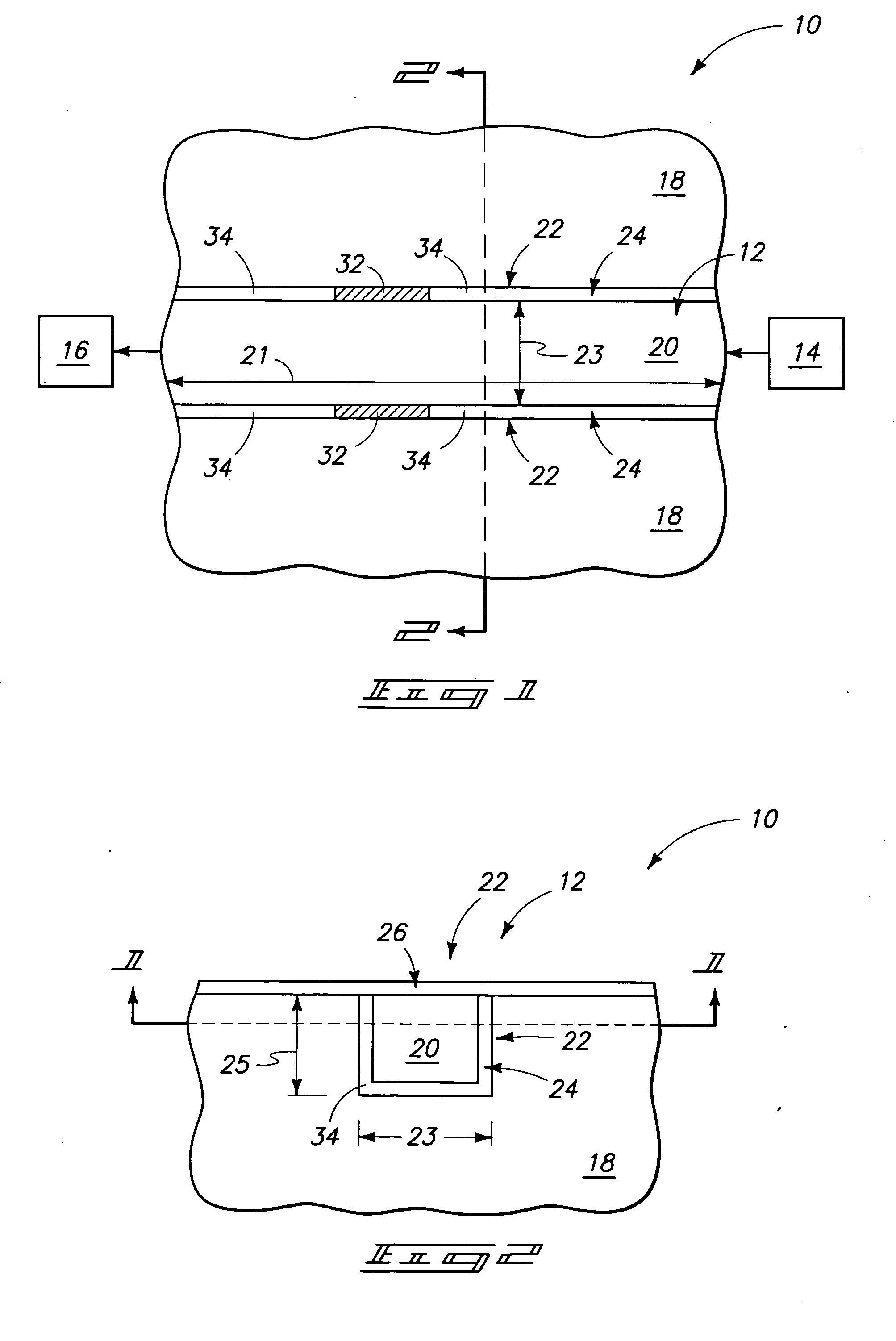
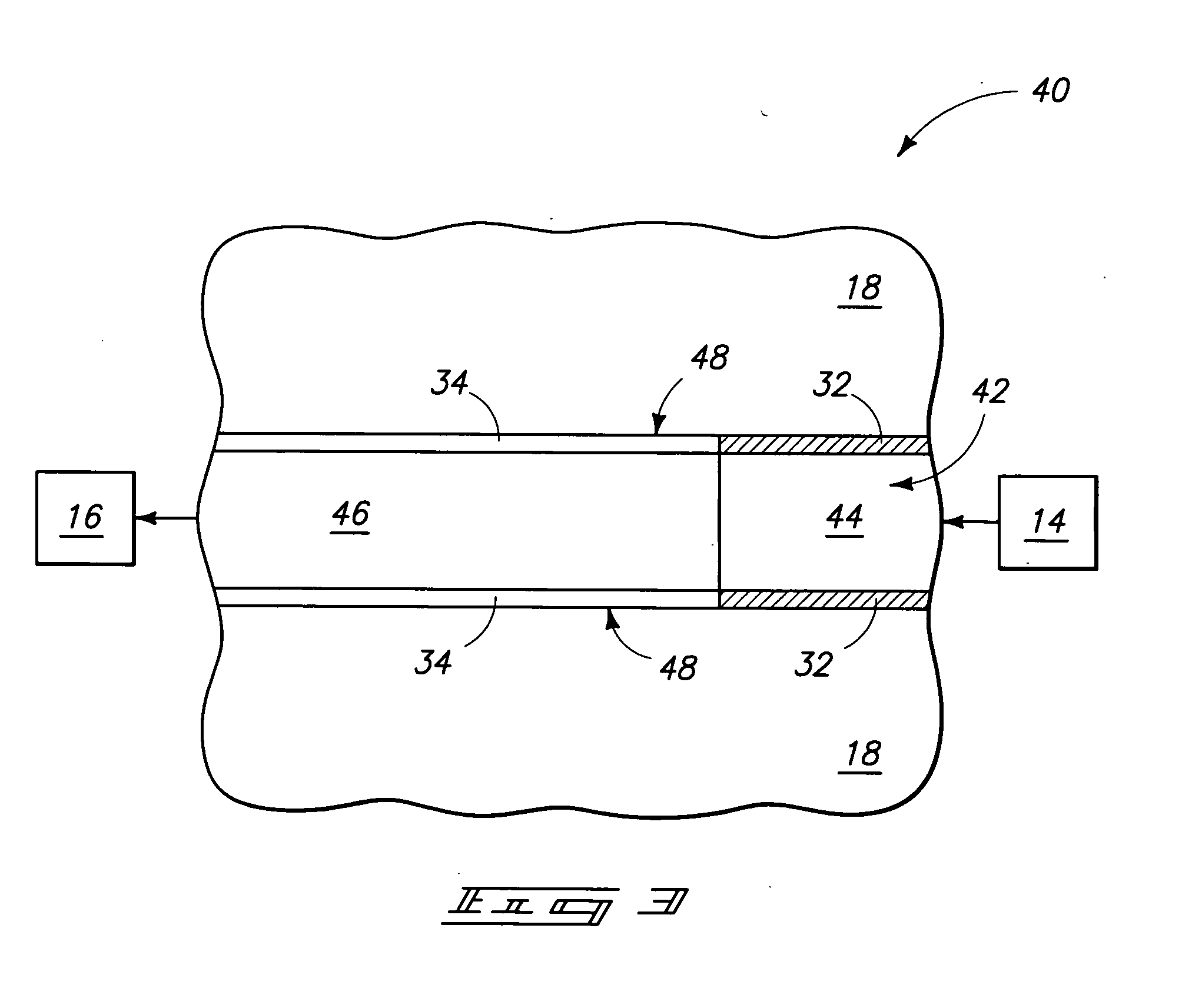
[0022] The invention includes optical waveguides and optical amplifiers, and methods of forming optical waveguides and optical amplifiers. In some aspects of the invention, it is recognized that rare earth elements can be utilized to amplify optical signals. The rare earth elements can be incorporated into optical interconnects, and in particular aspects into integrated circuit optical interconnects, to maintain signal strength of optical signals migrating along the optical interconnects. In some aspects, the rare earth elements can be utilized to amplify optical signal strength within at least a segment of an optical interconnect.

[0023] In some aspects, the rare earth elements can be considered to be incorporated within light-conducting conduits, with the term “light-conducting condui...


PUM


Abstract

The invention includes optical signal conduits having rare earth elements incorporated therein. The optical signal conduits can, for example, contain rare earth elements incorporated within a dielectric material matrix. For instance, erbium or cerium can be within silicon nanocrystals dispersed throughout dielectric material of optical signal conduits. The dielectric material can define a path for the optical signal, and can be wrapped in a sheath which aids in keeping the optical signal along the path. The sheath can include any suitable barrier material, and can, for example, contain one or more metallic materials. The invention also includes methods of forming optical signal conduits, with some of such methods being methods in which the optical signal conduits are formed to be part of semiconductor constructions.

Description

TECHNICAL FIELD [0001] The invention pertains to semiconductor constructions, methods of forming semiconductor constructions, light-conducting conduits, and optical signal propagation assemblies. BACKGROUND OF THE INVENTION [0002] There are many applications for optical signals. For instance, optical signals are frequently utilized for transferring data across large distances. Light conducting conduits (such as, for example, fiber optic cables) can be utilized as pathways for the optical signals. The optical signals can, however, become degraded during their travel from one point to another, and accordingly it can be desired to refresh the optical signals at various intervals along the pathways of the signals. [0003] Another use of optical signals is in ultra-fast computers. At very high frequencies, numerous physical effects degrade performance of electrons as dependable carriers of information, rendering the electrons incapable of being utilized for transferring information at ult...

Claims


Application Information

Patent Timeline
Patent Type & Authority Applications(United States)
IPC IPC(8): G02B6/10H01S3/00
CPCG02B6/10H01S3/0637H01S3/0632G02B6/12
Inventor MOULI, CHANDRA
Owner MICRON TECH INC
Why Eureka
Try Eureka