

Fabricating method for thin film transistor array substrate and thin film transistor array substrate using the same
a technology of thin film transistors and array substrates, which is applied in the direction of electrical equipment, semiconductor devices, instruments, etc., can solve the problems of current charged into the pixel electrodes b>18/b> by the channel, and the picture quality of the liquid crystal display device may be deteriorated, so as to prevent the effect of picture quality deterioration
- Summary
- Abstract
- Description
- Claims
- Application Information
AI Technical Summary
Benefits of technology
Problems solved by technology
Method used
Image


Examples
Embodiment Construction
[0060]Reference will now be made in detail to embodiments of the present invention, examples of which are illustrated in the accompanying drawings.
[0061]Hereinafter, embodiments of the present invention will be described in detail with reference to FIG. 4 to FIG. 8E.
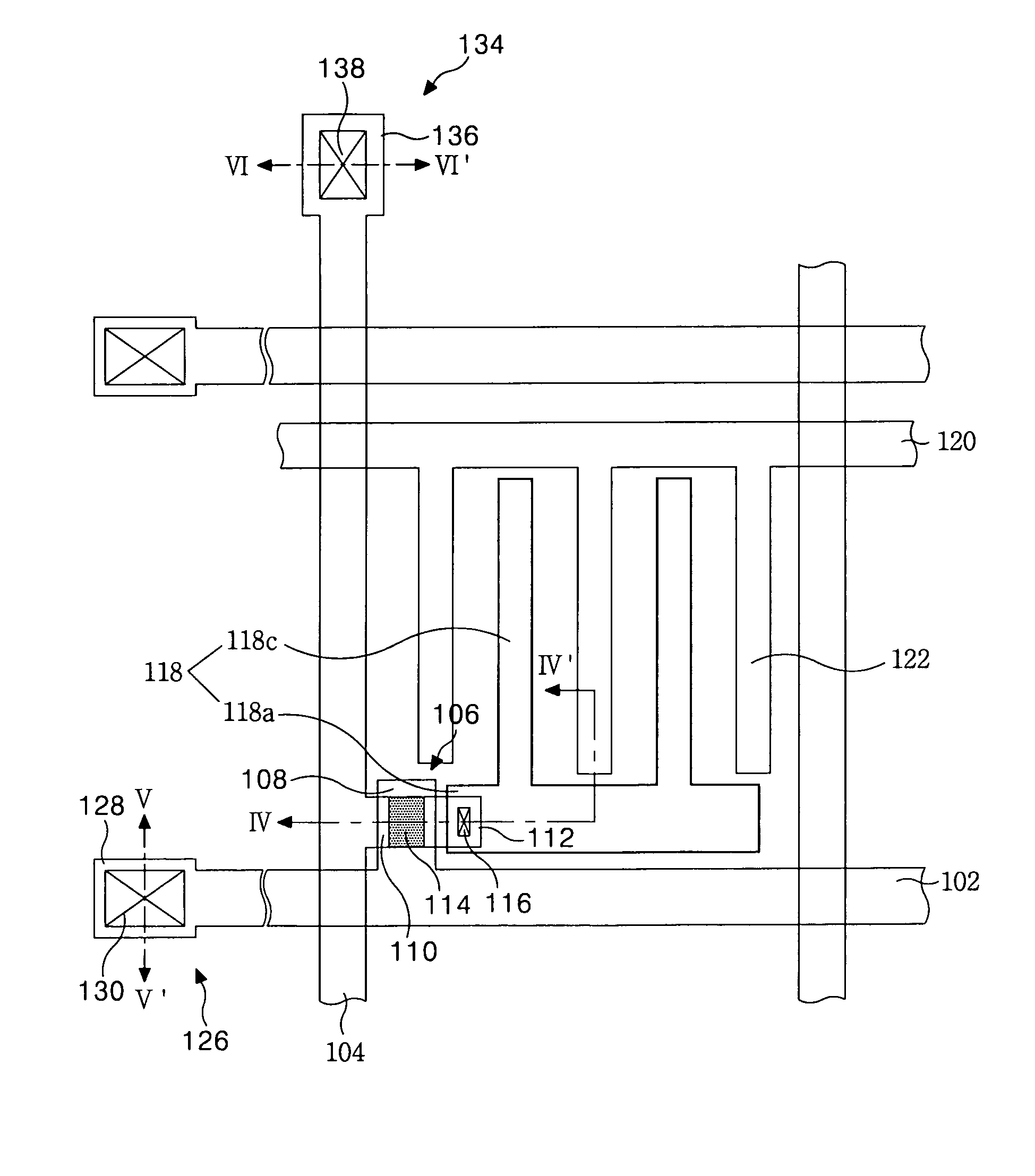
[0062]FIG. 4 is a plan view showing a thin film transistor array substrate according to an embodiment of the present invention, and FIG. 5 is a cross sectional view of the thin film transistor array substrate taken along the lines IV-IV′, V-V′ and VI-VI′ in FIG. 4.
[0063]Referring to FIG. 4 and FIG. 5, the TFT array substrate of the liquid crystal display device of horizontal electric field type according to an embodiment of the present invention includes a gate line 102 and a data line 104 provided on a lower substrate 142 in such a manner to intersect each other with a gate insulating film 144 therebetween, a TFT 106 provided at each intersection of the gate line 102 and the data line 104, a pixel electrode 118 and a co...
PUM
 Abstract
Description
Claims
Application Information