Method of producing semiconductor wafer

Inactive Publication Date: 2007-07-19
SUMCO CORP
View PDF6 Cites 100 Cited by
  • Summary
  • Abstract
  • Description
  • Claims
  • Application Information

AI Technical Summary

Benefits of technology

[0018](8) A method of producing a semiconductor wafer according to any one of the items (1)-(7), wherein the SiGe layer before the heat treatment has a maximum value of Ge concentration of not more than 30 mass %.
[0019](9) A method of producing a semiconductor wafer according to any one of the items (1)-(8), wherein the SiGe layer before the heat treatment has a gradient of Ge concentration of not more t

Problems solved by technology

However, in case of a region having a gate length of not more than 100 nm, the above establishment becomes difficult.
In this method, however, the SiGe layer of not less than few μm is interposed between the buried oxide film and the active layer as the channel layer for reducing defects, so that the superiority of the SOI substrate structure can not be developed sufficiently.
In this method, however, the strain in the SiGe layer can not be relaxed sufficiently and also the sufficient str

Method used


Image

  • Method of producing semiconductor wafer
  • Method of producing semiconductor wafer
  • Method of producing semiconductor wafer

Examples


example 1

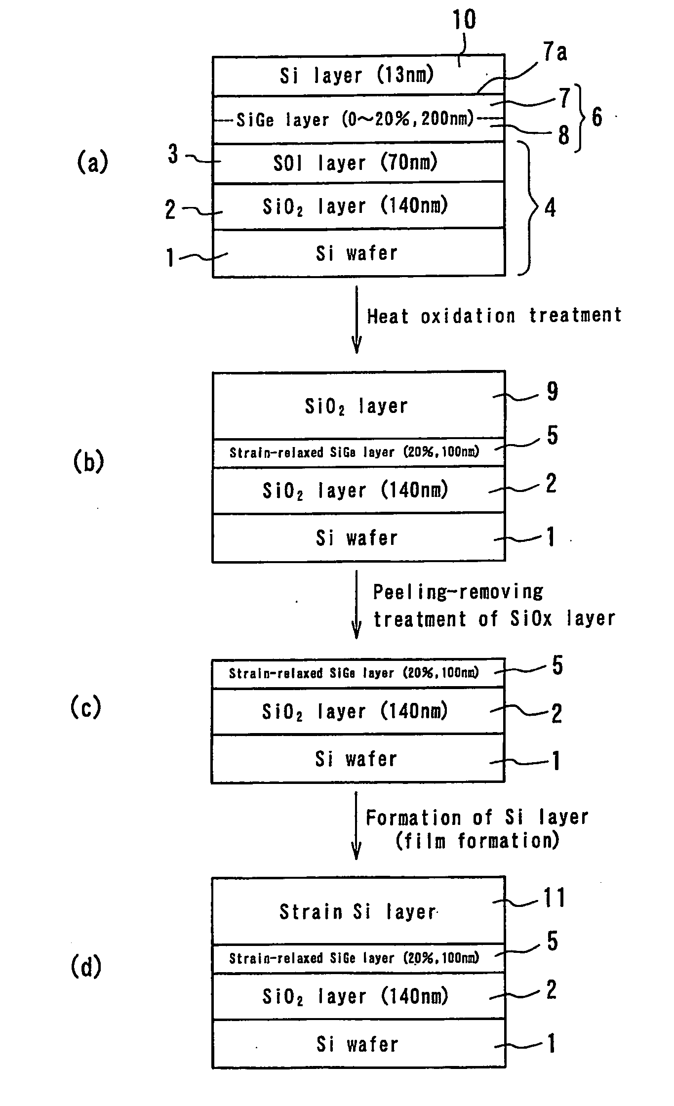
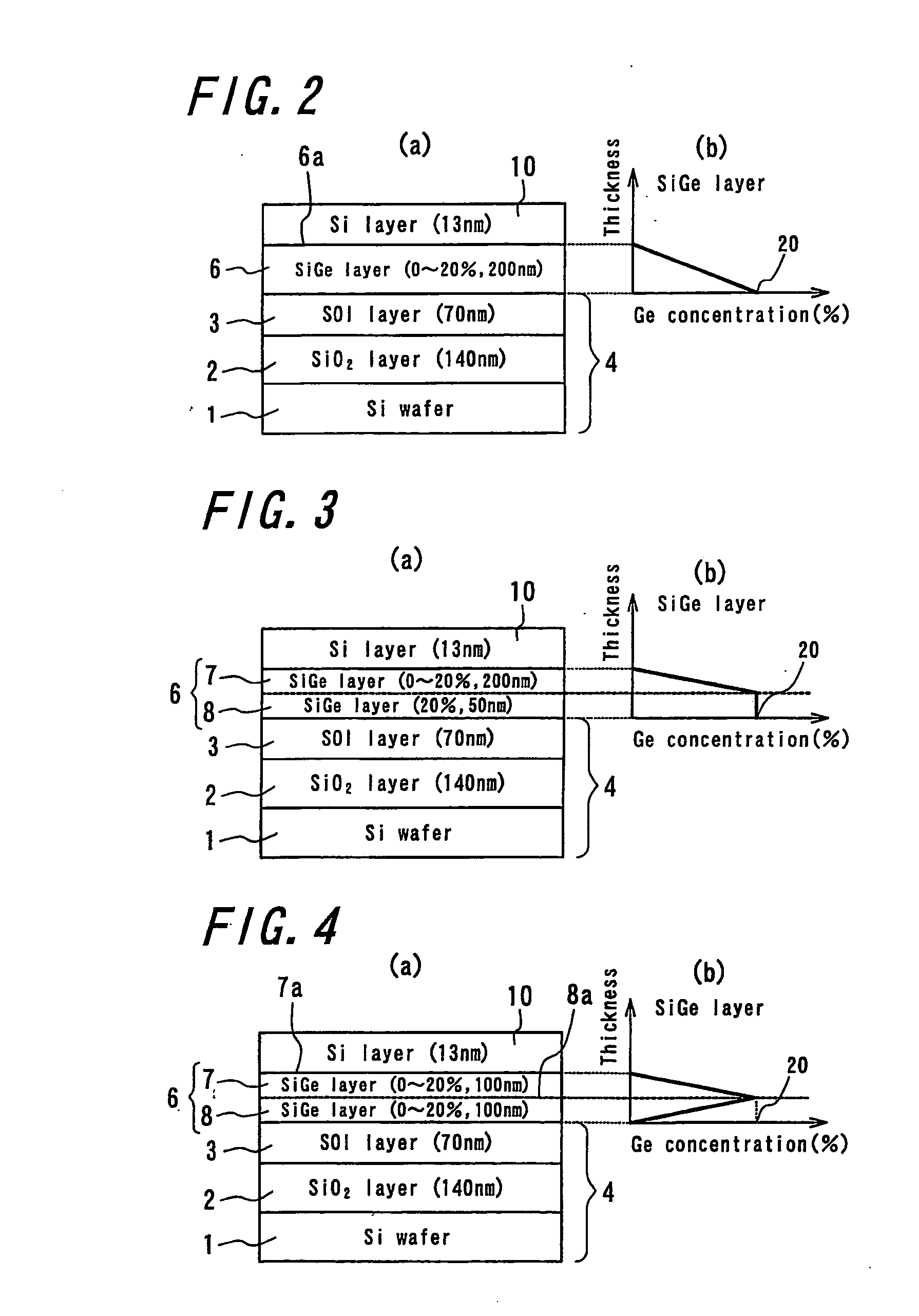
[0047]In a chamber of a CVD apparatus is placed a SOI wafer 4 and then a single crystal SiGe layer 6 is formed the SOI wafer 4 at a state of heating and keeping the SOI wafer 4 at 700° C. so that a Ge concentration is gradually decreased toward a surface while controlling a flow amount of a gas as a Ge source as shown in FIGS. 2(a) and (b). In this case, a maximum value of Ge concentration in the SiGe layer 6 is 20 mass % and a thickness is 200 nm. Then, a Si layer 10 is formed on the single crystal SiGe layer 6 at a thickness of 13 nm in the CVD apparatus, and thereafter the wafer provided with the Si layer 10 is subjected to a heat treatment in an oxidizing atmosphere of 100% oxygen at 1250° C. for 180 minutes to conduct the oxidation of wafer surface and diffusion of Ge to thereby form a strain-relaxed SiGe layer 5 having a thickness of 100 nm. In this case, the Ge concentration in the strain-relaxed SiGe layer 5 is 20 mass %. Thereafter, a SiO2 layer 9 formed at the surface is p...

example 2

[0048]In a chamber of a CVD apparatus is placed a SOI wafer 4 and then a portion 8 of a SiGe layer facing the SOI wafer is formed at a uniform Ge concentration (20 mass %) on the SOI wafer 4 at a state of heating and keeping the SOI wafer 4 at 700° C. while controlling a flow amount of a gas as a Ge source and further an upper layer side portion 7 of the SiGe layer 6 is formed so that the Ge concentration is 20 mass % at maximum and is gradually decreased toward a surface (Ge concentration: 0 mass %) as shown in FIGS. 3(a) and (b). In this case, the thickness of the portion 8 of the SiGe layer 6 facing the SOI wafer is 50 nm and the thickness of the upper layer side portion 7 of the SiGe layer 6 is 100 nm. The production steps other than the above are the same as in Example 1.

example 3

[0049]In a chamber of a CVD apparatus is placed a SOI wafer 4 and then a portion 8 of a SiGe layer facing the SOI wafer is formed on the SOI wafer 4 at a state of heating and keeping the SOI wafer 4 at 700° C. so that a Ge concentration is gradually increased toward a surface 8a (Ge concentration: 20 mass %) while controlling a flow amount of a gas as a Ge source and further an upper layer side portion 7 of the SiGe layer 6 is formed so that the Ge concentration is gradually decreased toward a surface 7a (Ge concentration: 0 mass %) while controlling the flow amount of the gas as a Ge source as shown in FIGS. 4(a) and (b). In this case, the thicknesses of the portion 8 of the SiGe layer 6 facing the SOI wafer and the upper layer side portion 7 of the SiGe layer 6 are 100 nm, respectively. The production steps other than the above are the same as in Example 1.


PUM


Abstract

A semiconductor wafer is produced at a step of forming a lattice relaxation or a partly lattice-relaxed strain relaxation SiGe layer on an insulating layer in a SOI wafer comprising an insulating layer and a SOI layer, wherein at least an upper layer side portion of the SiGe layer is formed on the SOI layer at a gradient of Ge concentration gradually decreasing toward the surface and then subjected to a heat treatment in an oxidizing atmosphere.

Description

BACKGROUND OF THE INVENTION[0001]1. Field of the Invention[0002]This invention relates to a method of producing a semiconductor wafer in which a lattice relaxation or a partly lattice-relaxed strain relaxation SiGe layer having a less defect and containing a uniform and high concentration of Ge can be formed on an insulating layer inside SOI wafer.[0003]2. Description of the Related Art[0004]In a silicon MOS device, the speeding-up and the low power consumption are established by conducting the scale down according to a scaling rule or the reduction of an operating voltage. However, in case of a region having a gate length of not more than 100 nm, the above establishment becomes difficult. For this end, an SOI substrate and an introduction of strained silicon are examined. Particularly, a substrate formed by introducing the strained silicon into the SOI substrate is considered as an ultimate substrate and studies thereof are going forward.[0005]In order to put such a substrate into ...

Claims


Application Information

Patent Timeline
IPC IPC(8): H01L21/336
CPCH01L21/02532H01L21/7624H01L21/0262
Inventor MATSUMOTO, KOJIHORA, TOMOYUKIENDO, AKIHIKOMORITA, ETSUROUNINOMIYA, MASAHARU
Owner SUMCO CORP
Why Eureka
Try Eureka