Photodetector with hetero-structure using lateral growth

a hetero-structure, optical detector technology, applied in the field of optical detectors, can solve the problems of limited optical applications, limited ge concentration of x/sub>alloy layer grown on silicon substrate, limited benefit of adding ge, etc., and achieves fast response, large lateral field, and high speed

Inactive Publication Date: 2005-06-16
IBM CORP
View PDF6 Cites 37 Cited by
  • Summary
  • Abstract
  • Description
  • Claims
  • Application Information

AI Technical Summary

Benefits of technology

[0004] The present invention describes a structure and method based on the lateral trench photodetector that enables high Ge concentration with deep light absorption depth. The lateral trench photodetector structure has advantages in that the lateral field is very large compared with a surface lateral p-i-n diode, enabling high speed, fast response and low supply voltage. See for instance, U.S. Pat No. 6,451,702 entitled: “Methods for forming lateral trench optical detectors” to M. Yang and K. Rim, incorporated herein by reference. In such a photodetector the light is incident from the top of the devices, and the electric field is in the lateral direction, transporting photocarriers laterally.
[0005] According to the present invention, a SiGe or Ge layer is introduced in the intrinsic region of a lateral trench detector, in such a manner that the depth of the absorption is not limited by the critical thickness of the Si1-xGex layer. This is achieved by using lateral epitaxial growth of the SiGe from the walls of a trench. The resulting photodetector by allowing an almost arbitrarily long photon absorption path in a high crystalline quality SiGe material, will have greatly improved capabilities in comparison to photodevices now in existence.

Problems solved by technology

However its optical applications are limited by its small light absorption coefficient due to its indirect band structure.
However due to the lattice mismatch between Si and Ge, to achieve defect-free quality the thickness of the Si1-xGex alloy layer grown on silicon substrate is limited by the Ge concentration, i.e. the higher the Ge content the thinner the Si1-xGex layer must be.
For application in shorter wavelength (for example 850 nm), although higher Ge content give larger light absorption coefficient compared with Si, the limited Si1-xGex thickness will limit the benefit of adding Ge.

Method used


Image

  • Photodetector with hetero-structure using lateral growth
  • Photodetector with hetero-structure using lateral growth
  • Photodetector with hetero-structure using lateral growth

Examples


Embodiment Construction

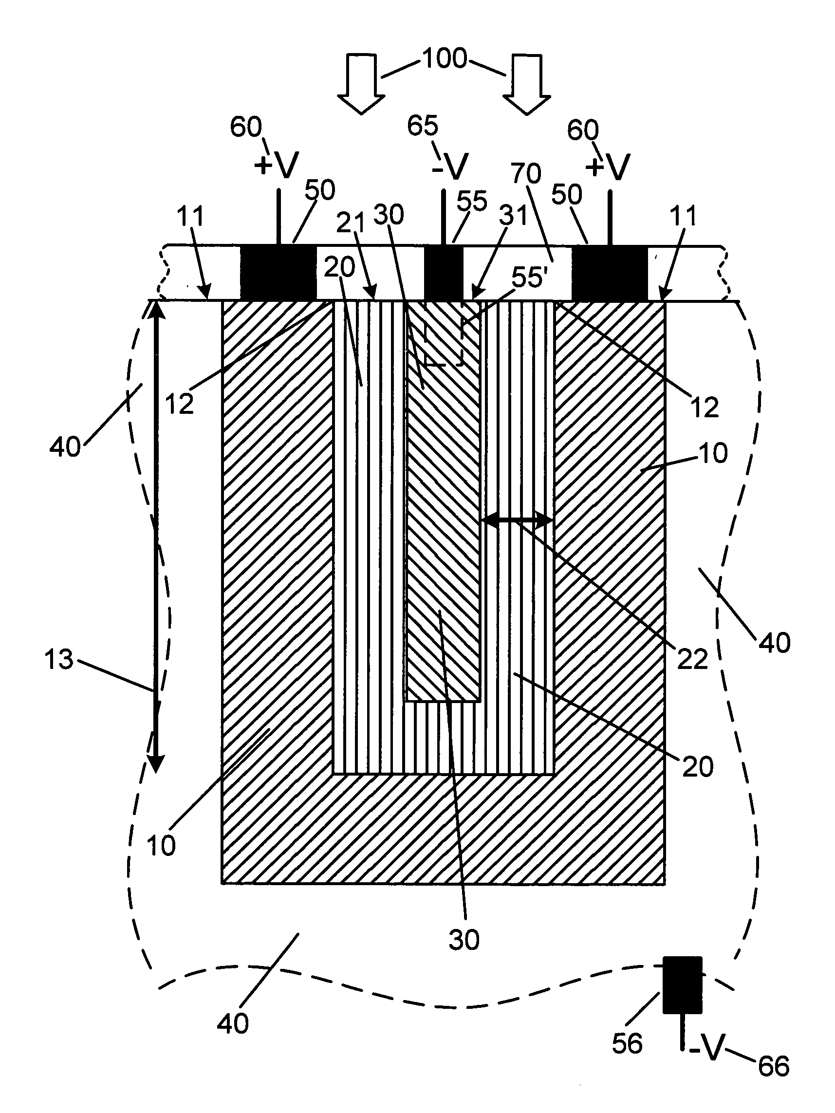
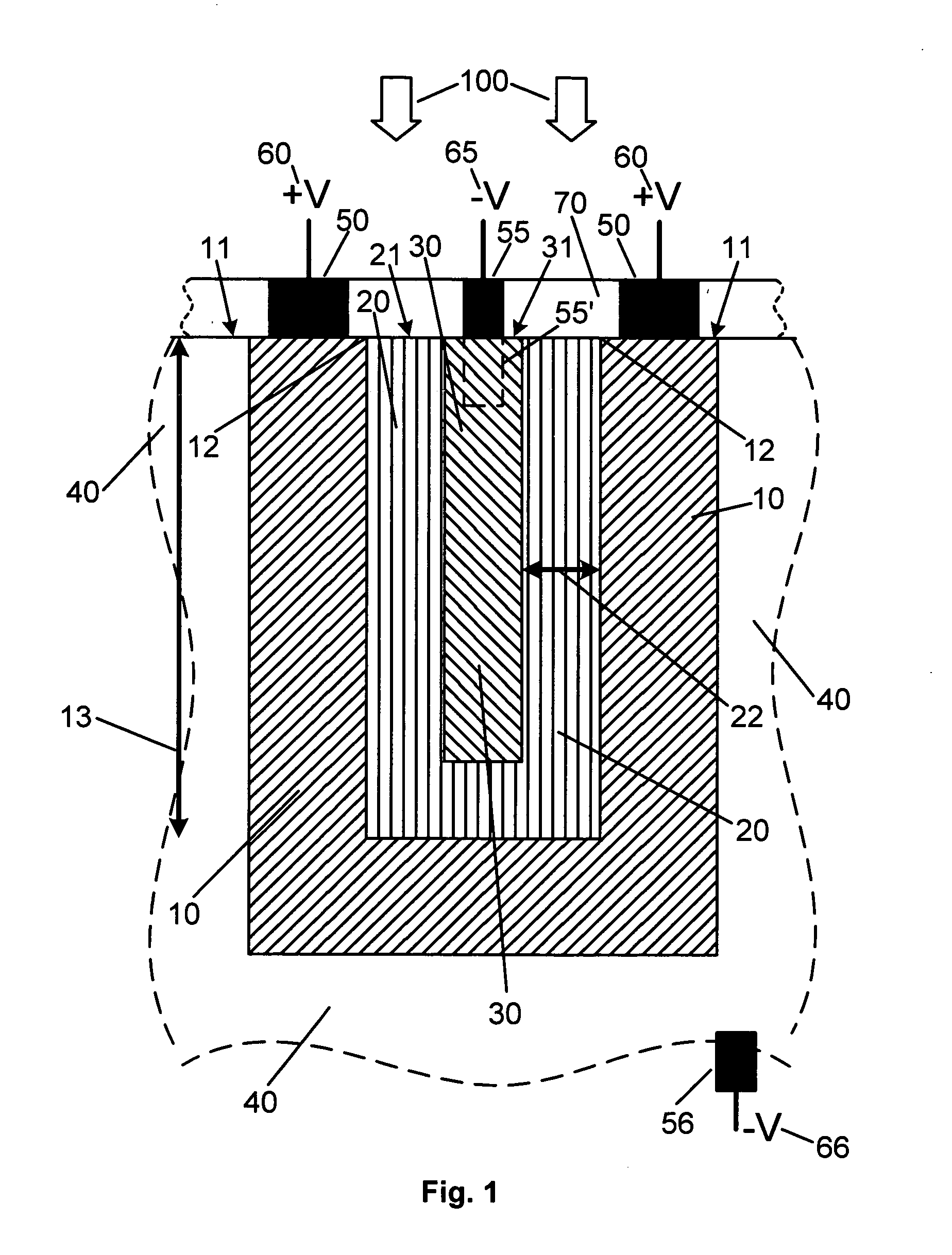
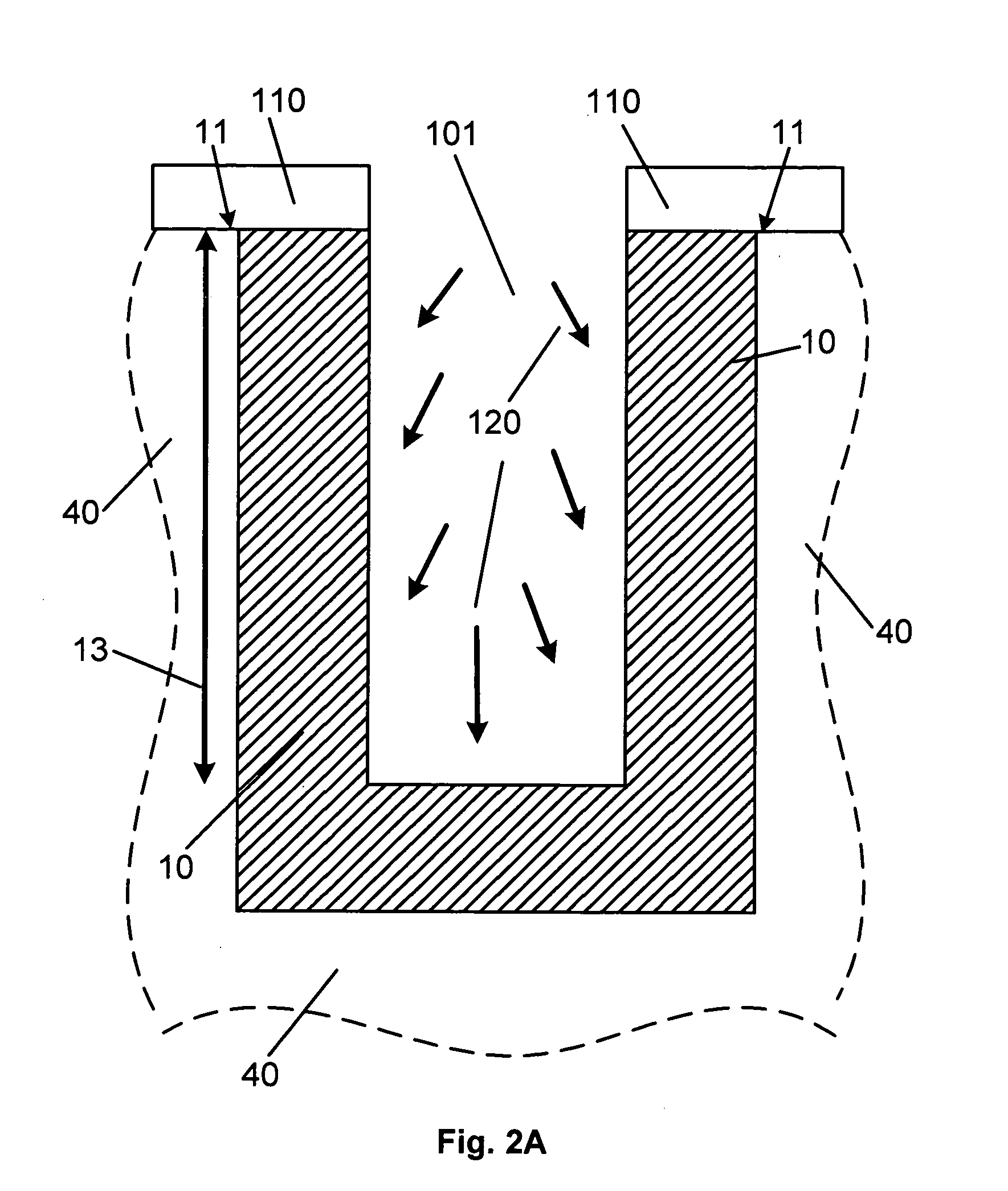
[0010]FIG. 1 schematically shows in cross section an exemplary embodiment of a heterojunction photodetector. A silicon (Si) body 40, typically with dimensions larger than the photodetector, (hence only a dotted outline is shown on FIG. 1), contains a Si well 10. The body 40 and well 10 are of the same material. The distinction, when there is any, between the two is in their doping. The well is heavily doped, to a first doping level, in the range of >1018 / cm3, while the body usually has at least an order of magnitude lower doping, typically 17 / cm3. Both the body and the well are single crystal, or monocrystalline Si. In a representative embodiment the body is a Si wafer, such as customarily found in the microelectronics art.

[0011] The well 10 has a first doping level and a first conductivity type. In exemplary embodiments the first conductivity type can be either n-type or p-type. The well 10 has a surface plane 11, which is essentially the plane of the body. Contained in the well a...


PUM


Abstract

A structure and method of fabrication for a Si based material p-i-n photodetector is disclosed. The light is absorbed in an undoped layer containing SiGe or Ge in such a manner that the absorption length is not limited by a critical thickness of the SiGe or Ge layer. The result is achieved by growing the SiGe or Ge layer from the walls of a trench in monocrystalline Si using lateral epitaxial. A second, doped material is disposed over the undoped layer for biasing and photocarrier collection in the p-i-n diode.

Description

FIELD OF THE INVENTION [0001] The present invention generally relates to optical detectors, and more particularly to lateral trench optical detectors formed in a Si based material framework. BACKGROUND OF THE INVENTION [0002] In many advance applications there is a need to combine microelectronics with optical technologies. One cornerstone device in optical technologies is the photodetector, a device which converts a light signal into an electrical signal. The material ruling microelectronics is silicon (Si). However its optical applications are limited by its small light absorption coefficient due to its indirect band structure. Moreover the cut-off wavelength in silicon is about 1.1 μm corresponding to its band-gap of 1.12 eV at room temperature. To extend the light absorption to infrared regime, especially to 1.3 or 1.55 μm for medium or long distance communication, and / or increase light absorption, germanium (Ge) is usually introduced into silicon in the absorption region (for e...

Claims


Application Information

Patent Timeline
Patent Type & Authority Applications(United States)
IPC IPC(8): H01J40/14H01L31/00H01L31/0328H01L31/105H01L31/18
CPCH01L31/1055Y02E10/547H01L31/1804Y02E10/548Y02P70/50
Inventor YANG, MIN
Owner IBM CORP
Why Eureka
Try Eureka