Method for forming a semiconductor device

a semiconductor and device technology, applied in semiconductor devices, chemical vapor deposition coatings, coatings, etc., can solve the problems of enhancing the mobility and driving current of the metal-oxide-semiconductor (mos) transistor, and achieve the effect of reducing the difficulty of removing the spacer and the ion implantation performed afterwards

Active Publication Date: 2010-04-15
UNITED MICROELECTRONICS CORP
View PDF7 Cites 102 Cited by
  • Summary
  • Abstract
  • Description
  • Claims
  • Application Information

AI Technical Summary

Benefits of technology

[0012]According to the method for forming a semiconductor device provided by the present invention, the etching process is introduced to remove the first epitaxial layer till the a portion of the substrate is exposed, thus the second epitaxial layer is to be formed along the etched plane profile of the first epitaxial layer after the etching process. Since the Ge concentration of the second epitaxial layer is higher than that of the first epitaxial layer, facet angles of the two epitaxial layers are different, and thus the included angle between the horizontal plane and the inclined plane of the islanding structure of the second epitaxial layer is larger than that of the first epitaxial layer. Consequently, contact areas between the second epitaxial layer and the spacer are reduced, and thus difficulties during removing the spacers and ion implantation performed afterwards are also reduced.

Problems solved by technology

As semiconductor processes advance to 65-nm node and beyond, and with the progress of device miniaturization, enhancing carrier mobility and a driving current of a Metal-Oxide-Semiconductor (MOS) transistor has become a critical issue.
The islanding structure causes difficulties in following steps such as ion implantation or removing spacers, and eventually exerts influences upon the performance of the MOS transistor.

Method used


Image

  • Method for forming a semiconductor device
  • Method for forming a semiconductor device
  • Method for forming a semiconductor device

Examples


Embodiment Construction

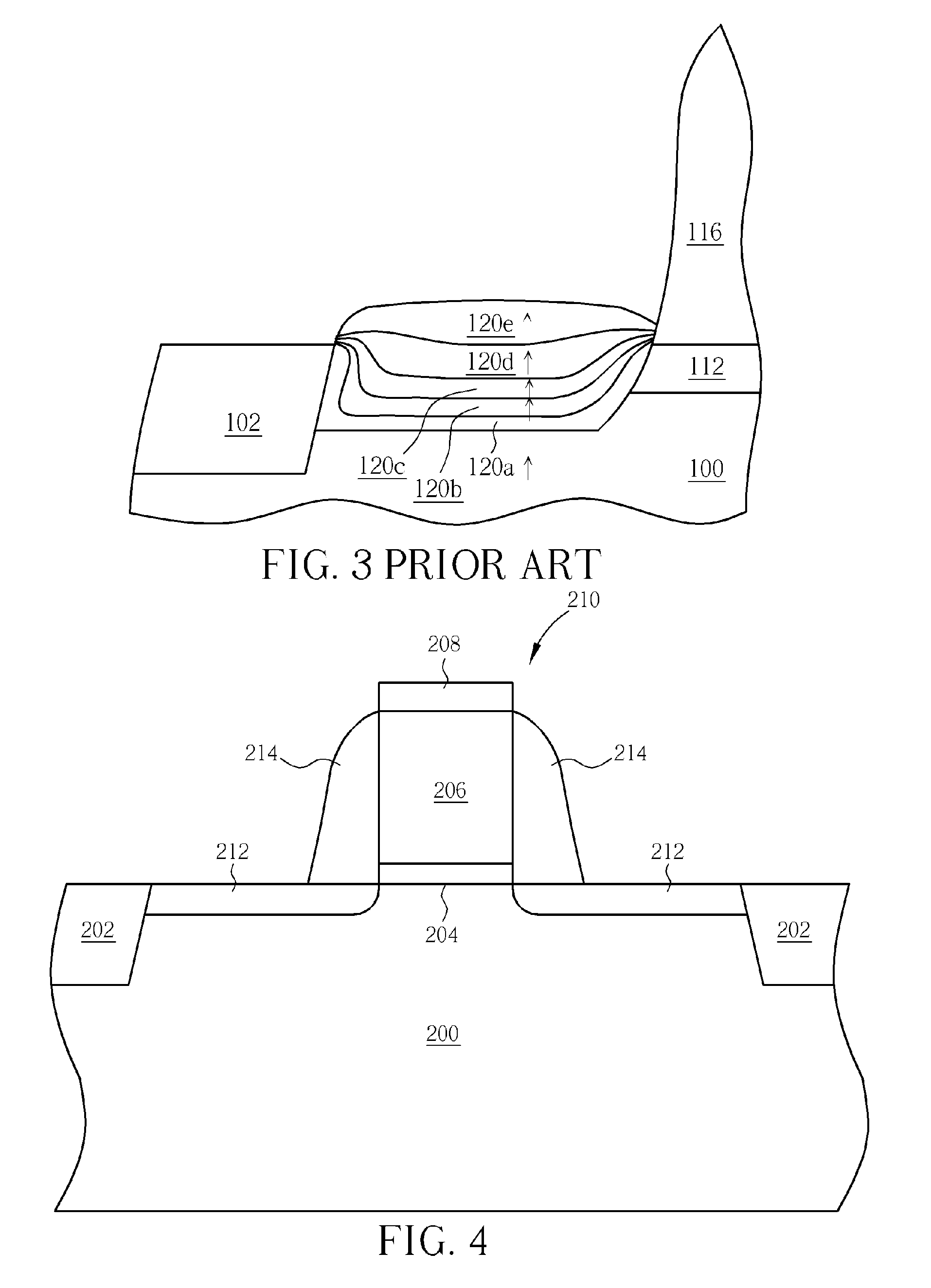
[0018]Please refer to FIGS. 4-8, which are schematic drawings illustrating a method for forming a semiconductor device according to a first preferred embodiment of the present invention. As shown in FIG. 4, a substrate 200, such as a silicon substrate, having a plurality of shallow trench isolation (STI) 202 serving for electrically isolating different semiconductor devices is provided. Then a patterned hard mask layer 208 used to define a gate dielectric layer 204 and a gate conductive layer 206 is formed, then a gate 210 is following formed.

[0019]Please refer to FIGS. 4-5. A first ion implantation is performed to form lightly doped drains (LDDs) 212 in the substrate 200 at two sides of the gate 210 and followed by forming a spacer 214 on sidewall of the gate 210. With the patterned hard mask layer 208 and the spacer 214 serving as masks during an etching process, recesses 216 are formed in the substrate 200 at two sides of the gate 210, as shown in FIG. 5.

[0020]Please refer to FIG...


PUM

PropertyMeasurementUnit
temperatureaaaaaaaaaa

Abstract

A method for forming a semiconductor device includes providing a substrate having at least a gate positioned thereon, forming at least a recess in the substrate adjacent to the gate, performing a first selective epitaxial growth (SEG) process to form a first epitaxial layer in the recess, performing an etching process to remove a portion of the first epitaxial layer to expose the substrate, and performing a second SEG process to form a second epitaxial layer on the first epitaxial layer.

Description

BACKGROUND OF THE INVENTION[0001]1. Field of the Invention[0002]The invention relates to a method for forming a semiconductor device, and more particularly, to a method for forming a semiconductor device with selective epitaxial growth (SEG) method.[0003]2. Description of the Prior Art[0004]As semiconductor processes advance to 65-nm node and beyond, and with the progress of device miniaturization, enhancing carrier mobility and a driving current of a Metal-Oxide-Semiconductor (MOS) transistor has become a critical issue. In order to improve a speed of the MOS transistor, a strained-silicon technique has been developed and is taken as a main solution to improve performance of the MOS transistor.[0005]One approach of the strained-silicon technique is applied with selective epitaxial growth (SEG) method, which involves forming an epitaxial layer, such as a SiGe layer, on a single-crystalline silicon substrate while the crystalline orientation of the epitaxial layer is almost identical...

Claims


Application Information

Patent Timeline
Patent Type & Authority Applications(United States)
IPC IPC(8): H01L21/336
CPCH01L21/28123H01L29/165H01L29/7834H01L29/7848H01L29/66636
Inventor LIAO, CHIN-ICHIEN, CHIN-CHENG
Owner UNITED MICROELECTRONICS CORP
Why Eureka
Try Eureka