
Capacitor and method for fabricating the same

Inactive Publication Date: 2007-07-26
SAMSUNG ELECTRONICS CO LTD
View PDF2 Cites 2 Cited by
  • Summary
  • Abstract
  • Description
  • Claims
  • Application Information

AI Technical Summary

Benefits of technology

[0011]Example embodiments provide a capacitor improvi

Problems solved by technology

Therefore, it may be difficult to obtain effective capacitance of the capacitor.
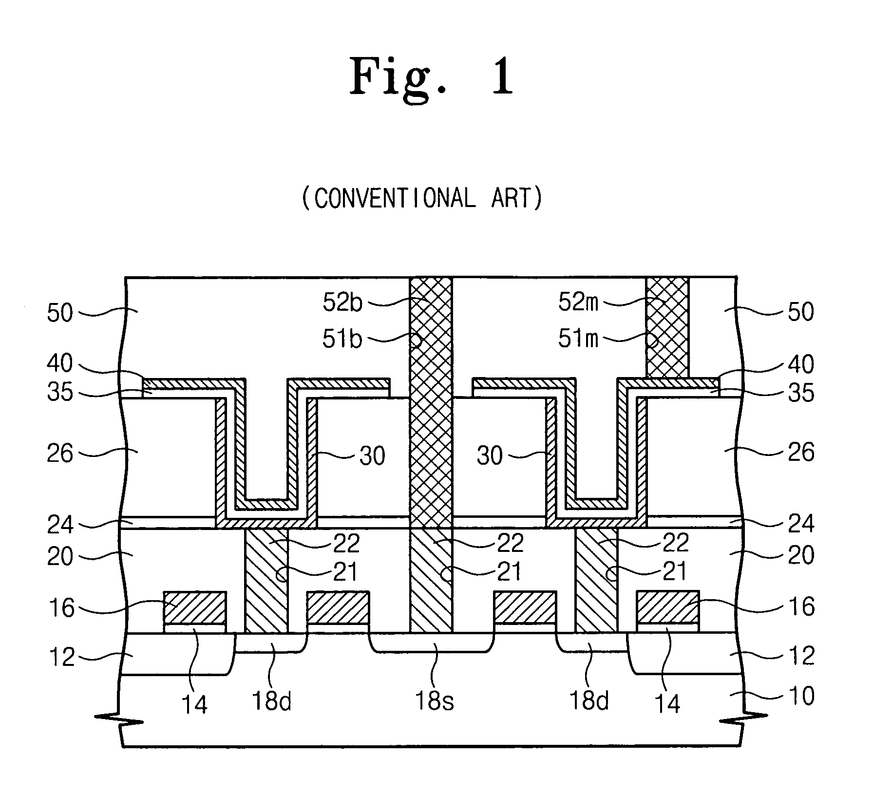
Due to CUB structure characteristics, when the height of the capacitor is increased to obtain more capacitance, there may be limitations in forming contact holes for a bit-line contact during an etching process and in forming a contact plug.

Method used


Image

  • Capacitor and method for fabricating the same
  • Capacitor and method for fabricating the same
  • Capacitor and method for fabricating the same

Examples


Embodiment Construction

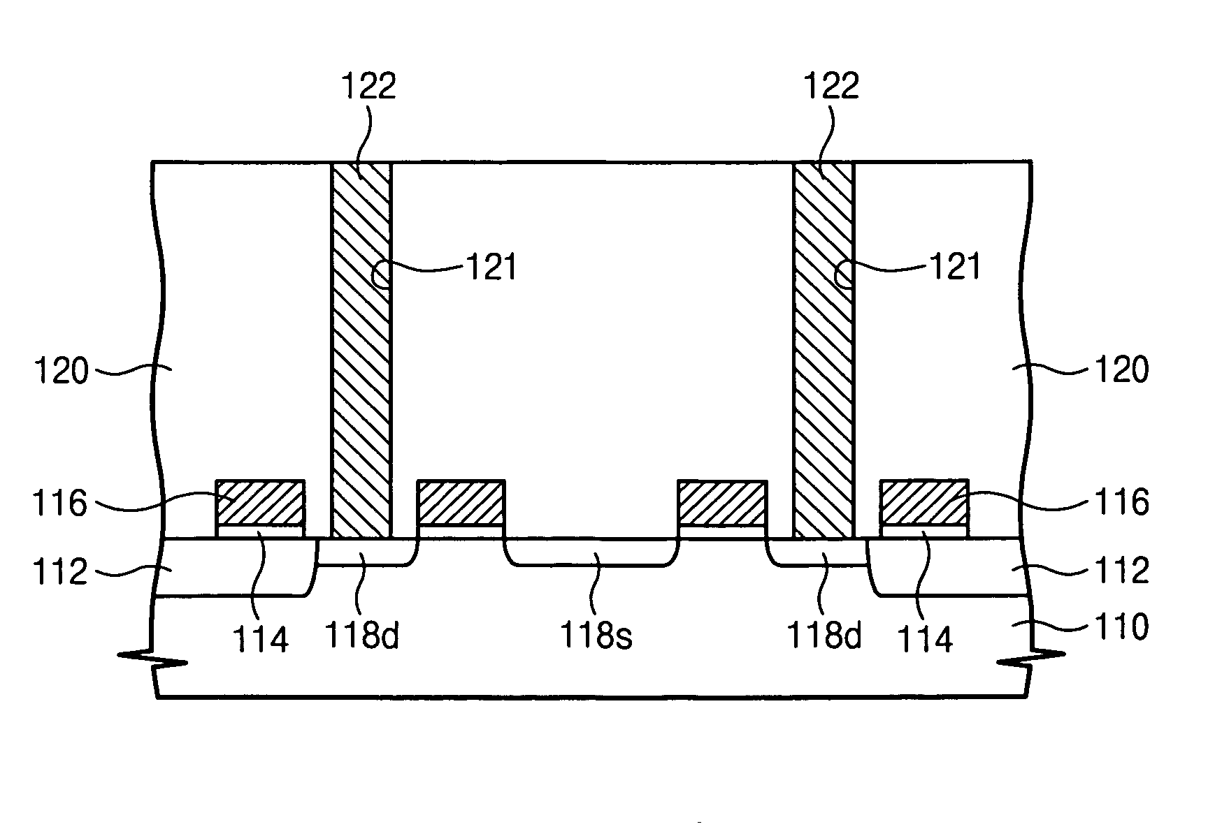
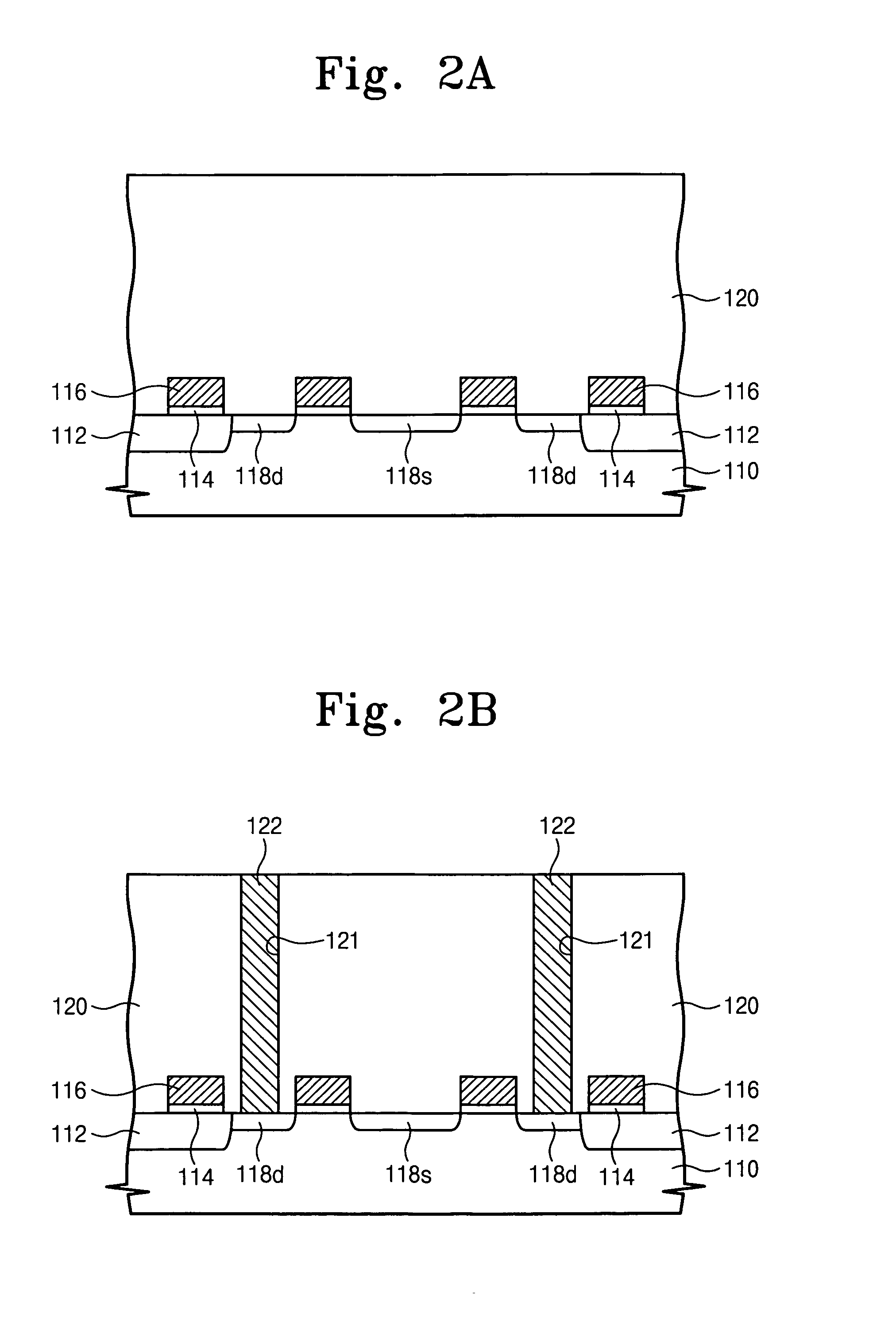
[0022]Reference will now be made in detail to the example embodiments, examples of which are illustrated in the accompanying drawings. However, example embodiments are not limited to the embodiments illustrated herein after, and the example embodiments herein are rather introduced to provide easy and complete understanding of the scope and spirit of example embodiments. In the drawings, the thicknesses of layers and regions are exaggerated for clarity. It will also be understood that when a layer is referred to as being “on” another layer or substrate, it may be directly on the other layer or substrate, or intervening layers may also be present. Like reference numerals in the drawings denote like elements, and thus their detailed description will be omitted for conciseness.

[0023]Spatially relative terms, such as “beneath,”“below,”“lower,”“above,”“upper” and the like, may be used herein for ease of description to describe one element or feature's relationship to another element(s) or...


PUM


Abstract

There is provided a capacitor and a method for fabricating the same. The method may include forming an interlayer insulation layer on a semiconductor substrate, patterning the interlayer insulation layer to form a contact hole exposing a region of the semiconductor substrate and forming a contact plug by filling the contact hole, wherein a top of the contact plug may have a height identical to that of the interlayer insulation layer. The method may further include forming a recess on the interlayer insulation layer, the recess exposing a portion of the contact plug, forming a bottom electrode on an inner profile of the recess including sides of the contact plug and depositing a dielectric layer and a top electrode on a profile of the semiconductor substrate including the bottom electrode to form a capacitor.

Description

PRIORITY STATEMENT[0001]This application claims priority under 35 U.S.C. §119 to Korean Patent Application No. 10-2006-0018886, filed on Jan. 20, 2006, in the Korean Intellectual Property Office (KIPO), the entire contents of which are incorporated herein by reference.BACKGROUND[0002]1. Field[0003]Example embodiments relate to a capacitor and method for fabricating the same.[0004]2. Description of the Related Art[0005]Because semiconductor devices have become highly integrated, a region that unit devices occupy on a semiconductor wafer may be reduced and a region that a capacitor occupies may also be reduced. The capacitor may be used in memory devices (e.g., Dynamic Random Access Memory (DRAM) and / or Static Ram (SRAM)). The capacitor may include respectively opposite conductive layers and a dielectric layer between the conductive layers. The capacitor may require a predetermined or given level of capacitance.[0006]There have been many efforts to improve the capacitance of the capac...

Claims


Application Information

Patent Timeline
IPC IPC(8): H01L21/44
CPCH01L27/10817H01L28/82H01L27/10852H10B12/318H10B12/033E03C1/181
Inventor KIM, JEONG-LIMYOUN, KWAN-YOUNG
Owner SAMSUNG ELECTRONICS CO LTD
Learn More