Predicting IC manufacturing yield by considering both systematic and random intra-die process variations

a technology of manufacturing yield and intra-die variation, applied in the direction of total factory control, programme control, semiconductor/solid-state device details, etc., can solve the problems of significant significant decrease in manufacturing yield, and increase in manufacturing cost, so as to reduce computation complexity

Active Publication Date: 2007-07-26
SYNOPSYS INC
View PDF13 Cites 34 Cited by
  • Summary
  • Abstract
  • Description
  • Claims
  • Application Information

AI Technical Summary

Benefits of technology

[0021] In a further variation on this embodiment, the system predicts the manufacturing yield for the die by using “windows” to select only a subset of the tiles to analyze, and thereby to reduce computation complexity. More specifically, the system selects a window with a specific geometry and size which is larger than a single tile. Next, the system selects a first tile from the array of tiles which satisfies a criterion. The system then places a first instance of the window around the first tile and iteratively: (1) selects a tile from the array of tiles which also satisfies the criterion and is not covered by an instance of the window; (2) places a new instance the window around the tile; and (3) repeats the above two steps until the entire die is covered by instances of the window. Next, the system computes spatial correlations for the random variations between all of the selected tiles. Finally, the system obtains the manufacturing yield for the die based on the systematic variations, the random variations and the spatial correlation of the random variations between the selected tiles.

Problems solved by technology

On the flip side, the constant drive towards ever-decreasing feature sizes has led to a significant increase in manufacturing cost.
One of the main causes of this increase in manufacturing costs is a significant decrease in manufacturing yield due to manufacturing losses.
IC manufacturing processes typically involve complex physical and chemical interactions.
Because it is impossible to perfectly control these complex physical and chemical interactions, process parameters associated with these manufacturing processes tend to fluctuate around their nominal values, causing “process parameter variations.” Such process parameter variations can significantly reduce manufacturing yield.
This is a problem because conventional techniques for predicting yield do not consider these intra-die variations.
However, due to increasing die-size and more-significant random intra-die variations, the spatial correlations of the random variations between two intra-die locations are not perfect, but instead decrease with the distances between the locations.
These non-perfect correlations between intra-die locations can strongly affect the total manufacturing yield.
Unfortunately, neither random intra-die variations nor the associated spatial correlations of the random intra-die variations have been taken into account while predicting the IC manufacturing yield.

Method used


Image

  • Predicting IC manufacturing yield by considering both systematic and random intra-die process variations
  • Predicting IC manufacturing yield by considering both systematic and random intra-die process variations
  • Predicting IC manufacturing yield by considering both systematic and random intra-die process variations

Examples


example

Cu Thickness in Chemical Mechanical Planerization (CMP)

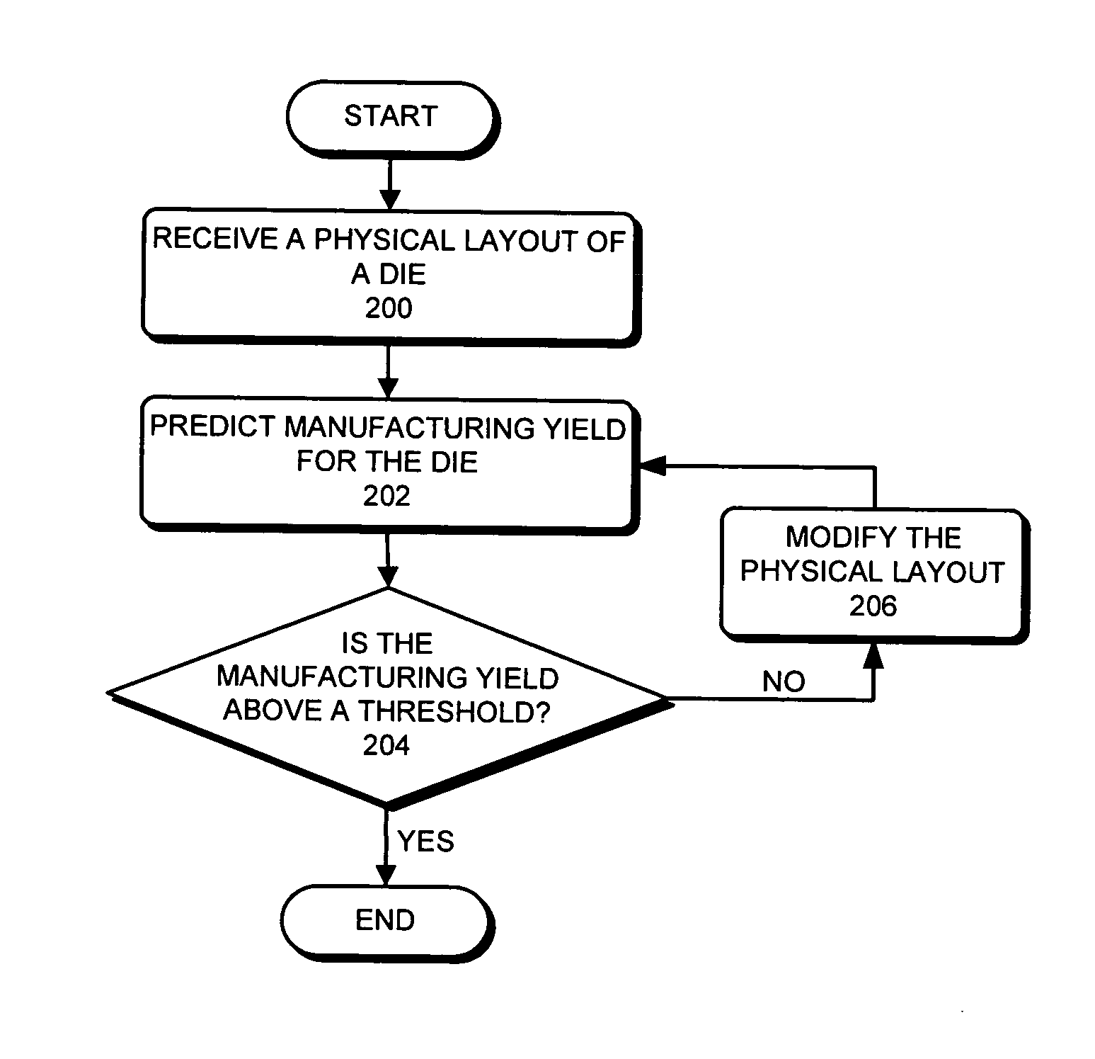
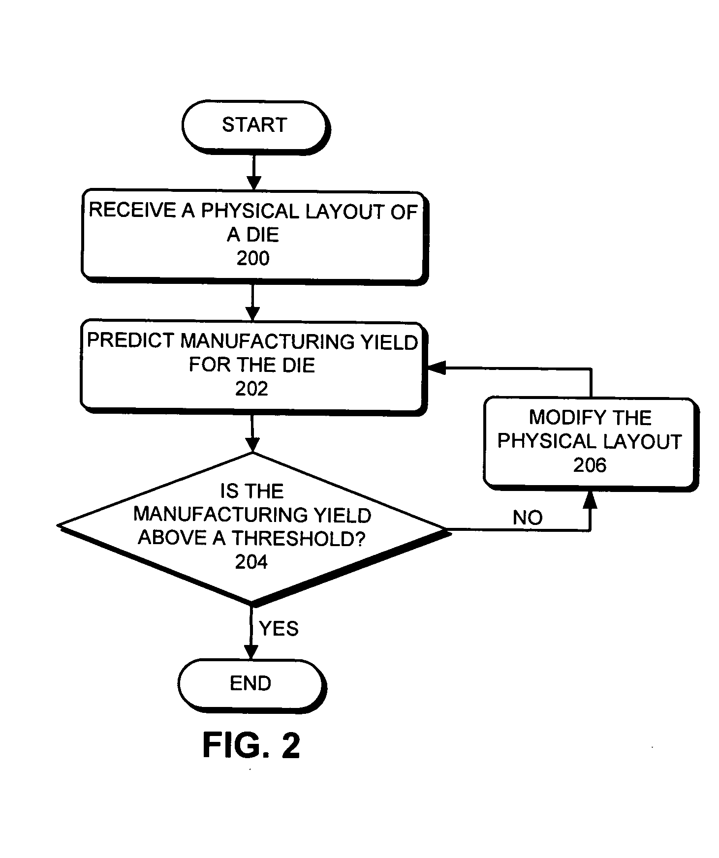
[0085] During IC manufacturing, a quality characteristic is often used to describe or monitor the quality of an IC fabrication process, such as the CD in a lithography process and Cu thickness in a CMP process. In the following discussion, Cu thickness in CMP is used as an example. However, the discussion below is also applicable to other IC manufacturing process parameters.

[0086] Ideally, a CMP process should yield a constant Cu thickness across a wafer. Practically, the Cu thickness at any given location on the wafer is affected by a number of process variables as well as design variables. The process variables can include the incoming Cu deposition thickness, barrier deposition thickness, Cu polishing rate, barrier polishing rate, CMP down pressure, velocity and so on. The design parameters can include the layout density, layout perimeter sum, line width and so on. All of these process and design parameters vary at differen...


PUM


Abstract

One embodiment of the present invention provides a system that predicts manufacturing yield for a die within a semiconductor wafer. During operation, the system first receives a physical layout of the die. Next, the system partitions the die into an array of tiles. The system then computes systematic variations for a quality indicative value to describe a process parameter across the array of tiles based on the physical layout of the die. Next, the system applies a random variation for the quality indicative parameter to each tile in the array of tiles. Finally, the system obtains the manufacturing yield for the die based on both the systematic variations and the random variations.

Description

BACKGROUND [0001] 1. Field of the Invention [0002] The present invention relates to techniques for predicting manufacturing yield for integrated circuit fabrication processes. More specifically, the present invention relates to a method and apparatus for predicting manufacturing yield for integrated circuit fabrication processes by considering both systematic and random intra-die variations. [0003] 2. Related Art [0004] Dramatic improvements in semiconductor integration circuit (IC) technology presently make it possible to integrate tens of millions of transistors, onto a single semiconductor IC chip. These improvements in integration densities have largely been achieved through corresponding improvements in semiconductor manufacturing technologies, which have recently achieved deep-submicron feature sizes. [0005] On the flip side, the constant drive towards ever-decreasing feature sizes has led to a significant increase in manufacturing cost. One of the main causes of this increase...

Claims


Application Information

Patent Timeline
Patent Type & Authority Applications(United States)
IPC IPC(8): G06F17/50
CPCG05B19/41875G05B2219/45031G05B2219/35142G05B2219/32204Y02P90/02
Inventor LUO, JIANFENGSINHA, SUBARNAREKHASU, QINGCHIANG, CHARLES C.
Owner SYNOPSYS INC
Why Eureka
Try Eureka