
Three-level nonvolatile semiconductor memory device and associated method of operation

Active Publication Date: 2007-08-02
SAMSUNG ELECTRONICS CO LTD
View PDF5 Cites 7 Cited by
  • Summary
  • Abstract
  • Description
  • Claims
  • Application Information

AI Technical Summary

Benefits of technology

[0015]Recognizing the limitations of conventional nonvolatile semiconductor memory devices, embodiments of the invention provide nonvolatile semiconductor devices and associated methods adapted to provide increased levels of integration and reliability relative to the conventional devices.

Problems solved by technology

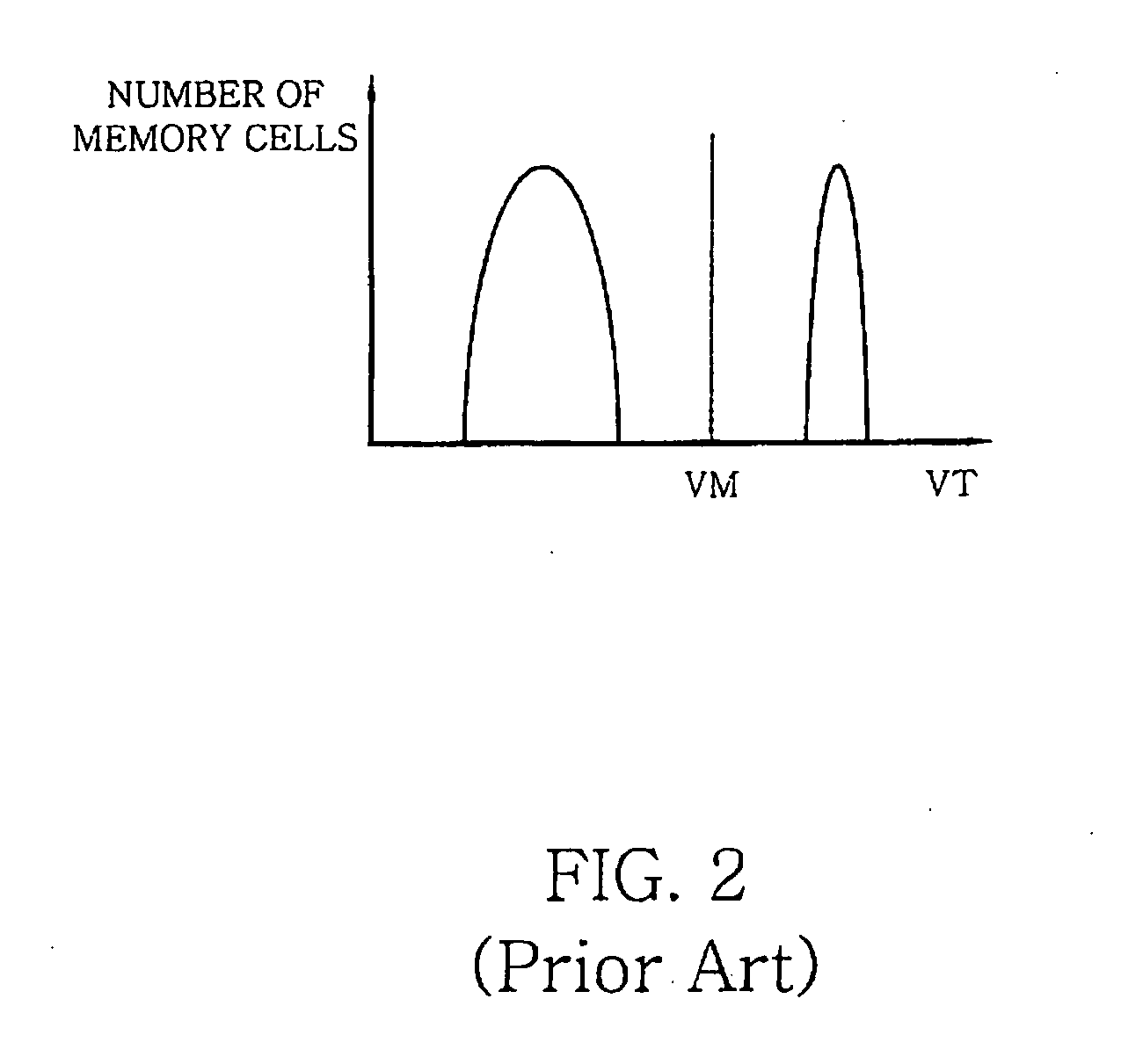
Accordingly, 4-level memory cells tend to be more susceptible to errors than 2-level memory cells due to shifts in the threshold voltage distributions.
These shifts can be caused, for example, by leakage currents.
Because the 4-level memory cells are more error prone than 2-level memory cells, the benefit of the additional storage capacity of the 4-level memory cells may be outweighed by their lack of reliability.

Method used


Image

  • Three-level nonvolatile semiconductor memory device and associated method of operation
  • Three-level nonvolatile semiconductor memory device and associated method of operation
  • Three-level nonvolatile semiconductor memory device and associated method of operation

Examples


Embodiment Construction

[0044]Exemplary embodiments of the invention are described below with reference to the corresponding drawings. These embodiments are presented as teaching examples. The actual scope of the invention is defined by the claims that follow.

[0045]Embodiments of the invention relate generally to nonvolatile semiconductor memory devices having 3-level memory cells. As an example, FIG. 4 illustrates threshold voltage distributions for a 3-level memory cell MC. The different threshold voltage distributions of FIG. 4 can be distinguished from each other in a read operation using first and second reference voltages VR1 and VR2.

[0046]In this written description, a threshold voltage distribution lower than first reference voltage VR1 will be referred to as a “first threshold voltage distribution G1”. A threshold voltage distribution between first reference voltage VR1 and second reference voltage VR2 will be referred to as a “second threshold voltage distribution G2”. Finally, a threshold voltag...


PUM


Abstract

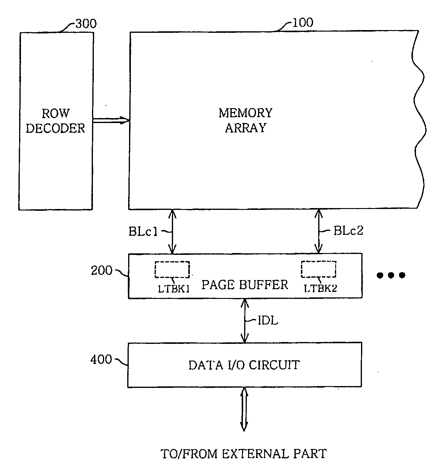
A nonvolatile semiconductor memory device comprises a memory array of 3-level nonvolatile memory cells. The memory array comprises first even and odd strings of memory cells connected to respective first even and odd bit lines and second even and odd strings of memory cells connected to respective second even and odd bit lines. The first even and odd bit lines are selectively connected to a first common bit line during data programming and read operations, and the second even and odd bit lines are selectively connected to a second common bit line during data programming and read operations. The device programs and reads data in a pair of memory cells using three bits of data corresponding to three threshold voltage distributions of the 3-level nonvolatile memory cells.

Description

BACKGROUND OF THE INVENTION[0001]1. Field of the Invention[0002]Embodiments of the invention relate generally to semiconductor memory devices. More particularly, embodiments of the invention relate to nonvolatile semiconductor memory devices having three-level memory cells, and methods of operating the nonvolatile semiconductor memory devices.[0003]This application claims priority to Korean Patent Application No. 10-2006-9631 filed on Feb. 1, 2006, the subject matter of which is incorporated by reference in its entirety.[0004]2. Description of Related Art[0005]Nonvolatile semiconductor memory devices retain stored data even when disconnected from an external power source. Accordingly, these types of memory devices are an especially popular way of providing long term data storage in electronic devices where power is limited or may be cut off, such as portable electronic devices.[0006]There are a wide variety of nonvolatile memory devices, including, for example, ferroelectric random ...

Claims


Application Information

Patent Timeline
IPC IPC(8): G11C7/10
CPCG11C7/18G11C11/5628G11C2211/5642G11C16/0483G11C11/5642A47G9/10
Inventor MO, HYUN-SUNKIM, HO-JUNG
Owner SAMSUNG ELECTRONICS CO LTD
Learn More