Thin film transistor substrate and method of manufacturing the same and mask for manufacturing thin film transistor substrate

a technology of thin film transistors and substrates, which is applied in the direction of semiconductor devices, instruments, electrical devices, etc., can solve the problem of generating a repeatable imag

Active Publication Date: 2007-08-09
SAMSUNG DISPLAY CO LTD
View PDF8 Cites 12 Cited by
  • Summary
  • Abstract
  • Description
  • Claims
  • Application Information

AI Technical Summary

Problems solved by technology

Thus, there is a problem in that a residual image may be generated if there is an increase in the off current.

Method used


Image

  • Thin film transistor substrate and method of manufacturing the same and mask for manufacturing thin film transistor substrate
  • Thin film transistor substrate and method of manufacturing the same and mask for manufacturing thin film transistor substrate
  • Thin film transistor substrate and method of manufacturing the same and mask for manufacturing thin film transistor substrate

Examples


Embodiment Construction

[0076]Hereinafter, exemplary embodiments of the present invention will be described in detail with reference to the accompanying drawings. However, the present invention is not limited to the embodiments but may be implemented into different forms. These embodiments are provided only for illustrative purposes and for full understanding of the scope of the present invention by those skilled in the art.

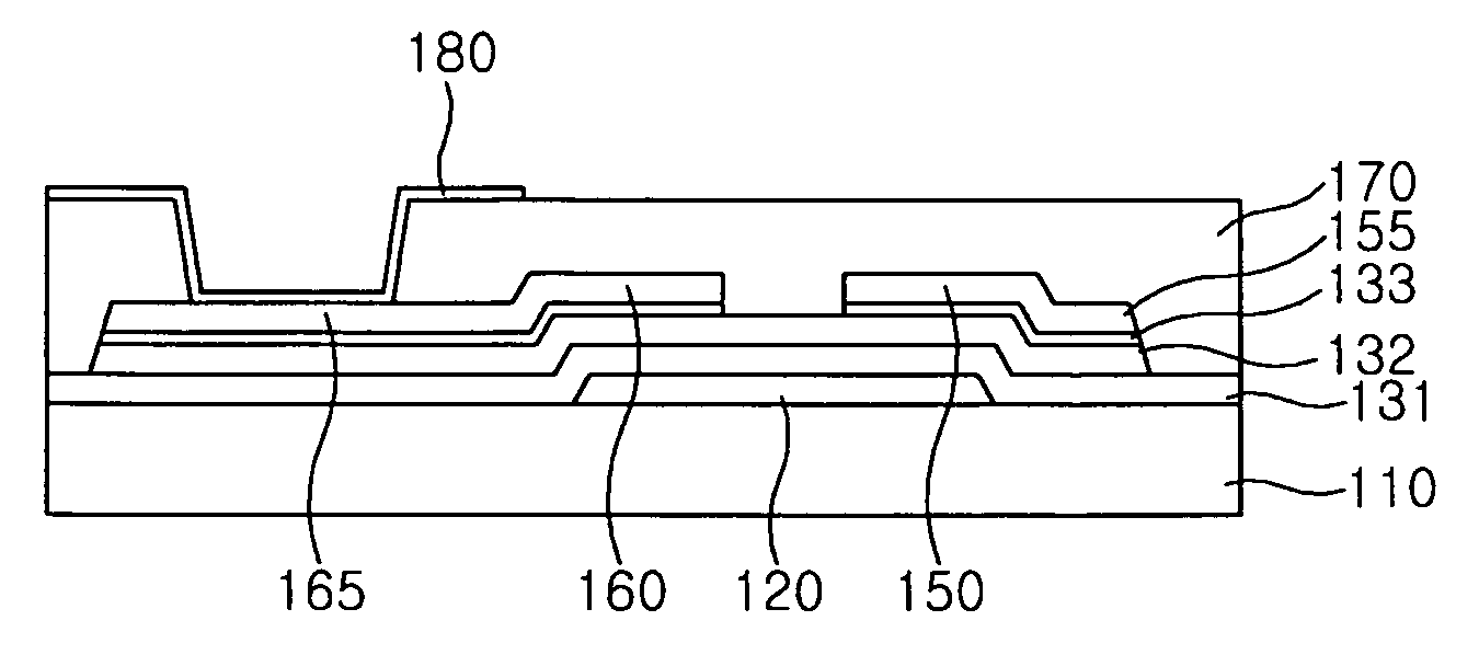
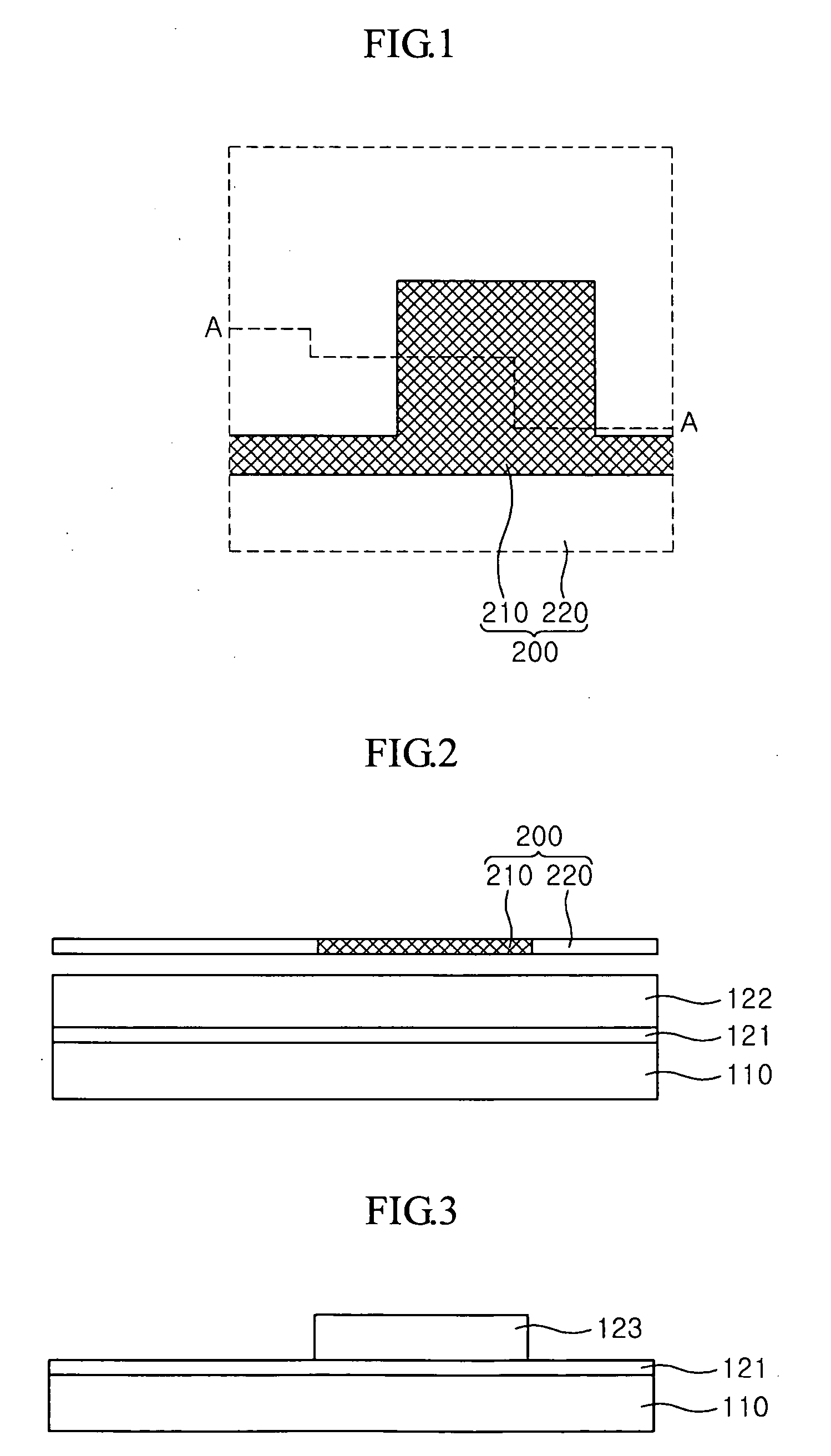
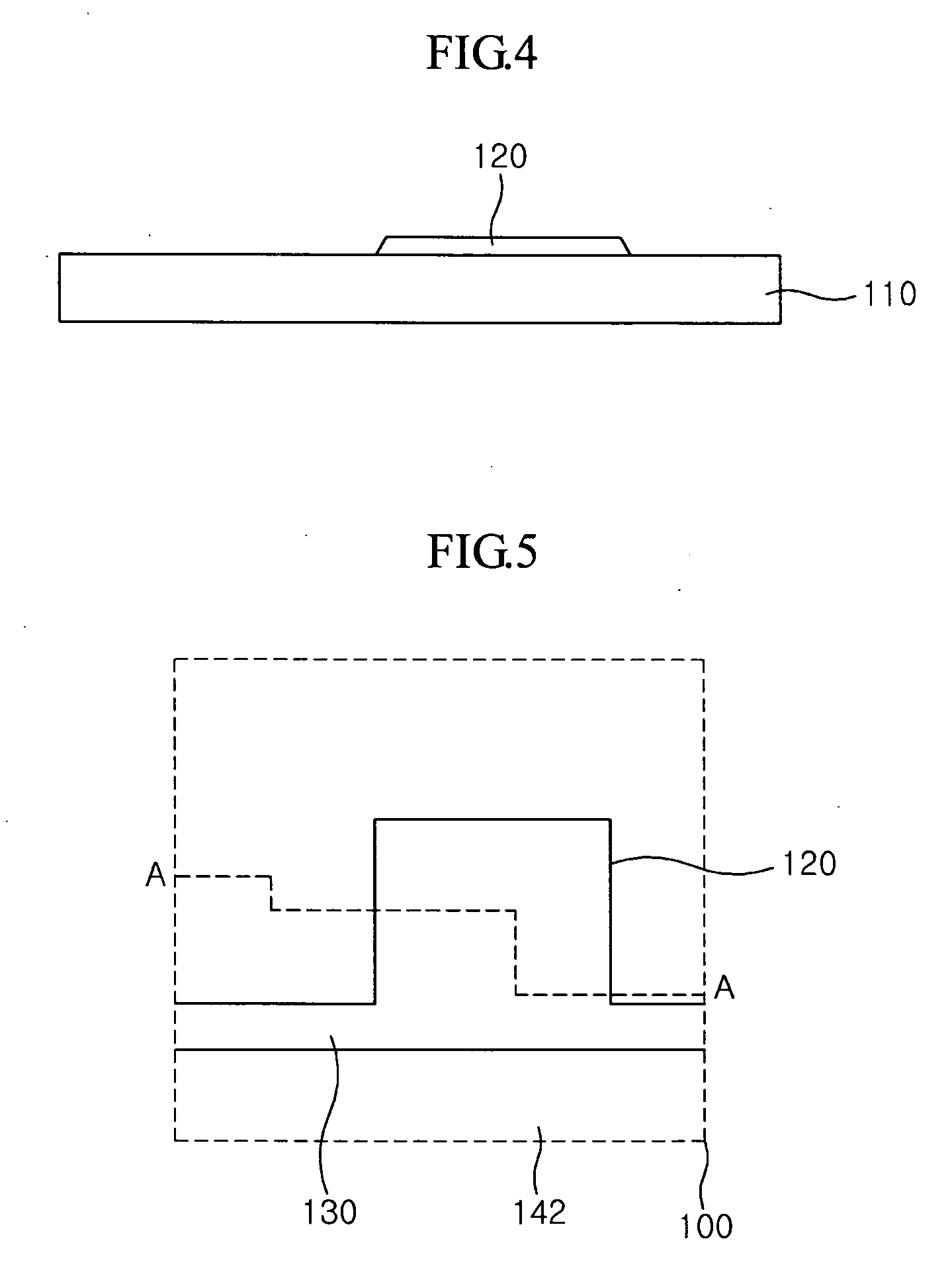
[0077]FIG. 1 is a plan view of a mask for forming a gate electrode according to an embodiment of the present invention, FIGS. 2 to 4 are sectional views taken along line A-A in FIG. 1 to illustrate the formation of the gate electrode, and FIG. 5 is a plan view of a substrate on which the gate electrode is formed.

[0078]The formation of the gate electrode will be described below with reference to FIGS. 1 to 5. As shown in FIG. 2, a first conductive film 121 is first formed on a transparent insulative substrate 110, and a first photosensitive film 122 is then applied thereon. The photosens...


PUM


Abstract

A thin film transistor substrate, wherein the moving area of electrons between source and drain electrodes of a thin film transistor (TFT) is minimized, the moving distance of electrons is increased, and the sizes of capacitors defined by a gate electrode together with the respective source and drain electrodes are identical to each other so that an off current generated when the TFT is off can be minimized; a method of manufacturing the thin film transistor substrate; and a mask for manufacturing the thin film transistor substrate. Accordingly, it is possible to minimize an off current induced due to a phenomenon of electron trapping by light.

Description

CROSS-REFERENCE TO RELATED APPLICATIONS[0001]The present application claims priority from Korean Patent Application No. 10-2006-0010831 filed Feb. 3, 2006 and No. 10-2006-0012147 filed Feb. 8, 2006, the disclosures of which are hereby incorporated by reference in their entirety.BACKGROUND OF THE INVENTION[0002]1. Technical Field[0003]The present disclosure relates to a thin film transistor substrate, a method of manufacturing the same, and a mask for manufacturing a thin film transistor substrate. More particularly, the present disclosure relates to a thin film transistor capable of minimizing an off current of the thin film transistor.[0004]2. Discussion of the Related Art[0005]In general, a liquid crystal display (LCD) comprises a thin film transistor substrate on which a pixel electrode, a storage capacitor, a thin film transistor (TFT) for switching each pixel, and the like are formed; a common electrode substrate on which a common electrode and the like are formed; and liquid c...

Claims


Application Information

Patent Timeline
Patent Type & Authority Applications(United States)
IPC IPC(8): H01L29/04
CPCH01L27/1288H01L27/1214H01L27/1222H01L27/124
Inventor LIM, DO GILEE, JONG HWANLEE, HONG WOOKIM, YONG JOLEE, YONG WOO
Owner SAMSUNG DISPLAY CO LTD
Why Eureka
Try Eureka