

Charge balance insulated gate bipolar transistor
- Summary
- Abstract
- Description
- Claims
- Application Information
AI Technical Summary
Problems solved by technology
Method used
Image

Examples
Embodiment Construction
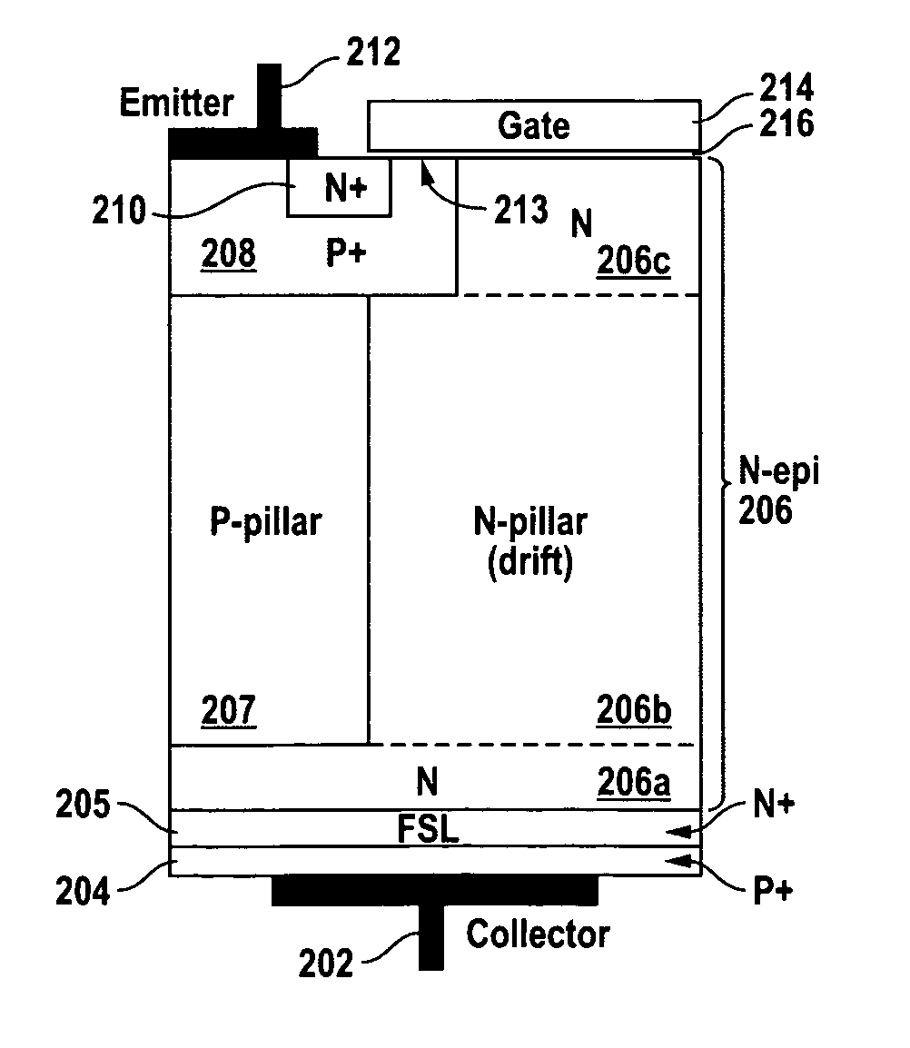
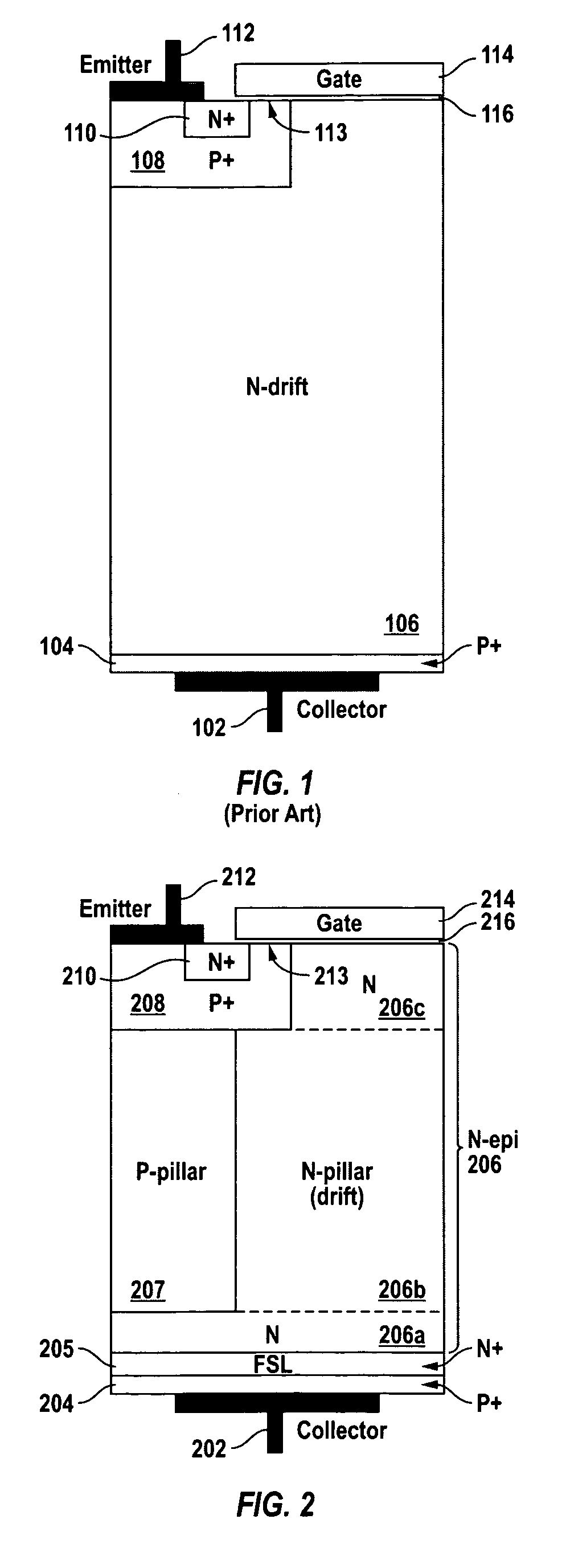
[0022]FIG. 2 is a cross section view of an improved superjunction IGBT which allows various competing performance parameters to be improved, in accordance with an embodiment of the invention. A highly doped P-type collector region 204 is electrically connected to a collector electrode 202. A N-type field stop layer (FSL) 205 extends over collector region 204, and an N-type region 206a extends over FSL 205. A charge balance region comprising alternating P-pillars 207 and N-pillars 206b extends over N-type region 206a. In an alternate embodiment, region 207 of the charge balance region comprises a P-type silicon liner extending along the vertical boundaries and the bottom boundary of region 207 with the remainder of region 207 being N-type or intrinsic silicon.
[0023] A highly doped P-type well region 208 extends over P-pillars 207, and a highly doped N-type source region 210 is formed in well region 208. Both well region 208 and source region 210 are electrically connected to an emit...
PUM
 Abstract
Description
Claims
Application Information