Impedance matching commonly and independently

a technology of impedance matching and common impedance, which is applied in the field of common impedance matching and independent impedance matching, can solve the problems of easy adjustment errors and troublesome operation, and achieve the effect of improving impedance matching with the transmission line and high accuracy impedance matching

US20070182601A1Inactive Publication Date: 2007-08-09RENESAS TECH CORP
4 Cites 4 Cited by

Patent Information

Authority / Receiving Office
US · United States
Patent Type
Applications(United States)
Current Assignee / Owner
Publication Date
2007-08-09
Estimated Expiration
Not applicable · inactive patent

Smart Images

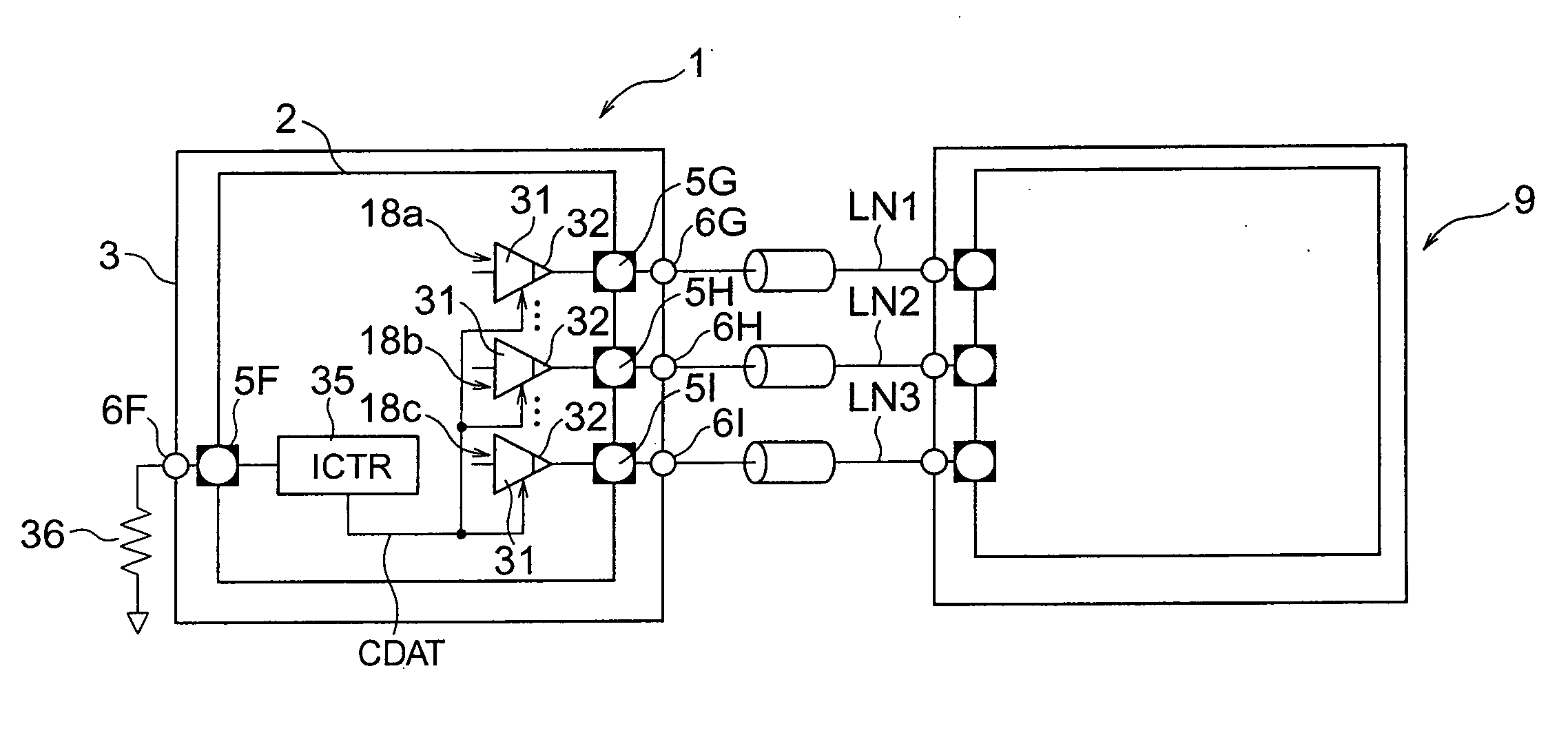
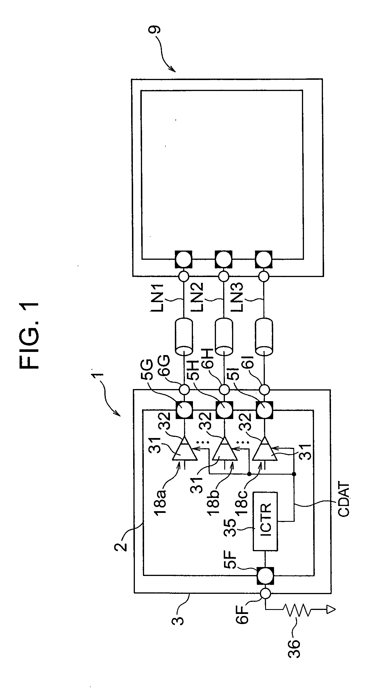
  • Figure 1
    Figure 1
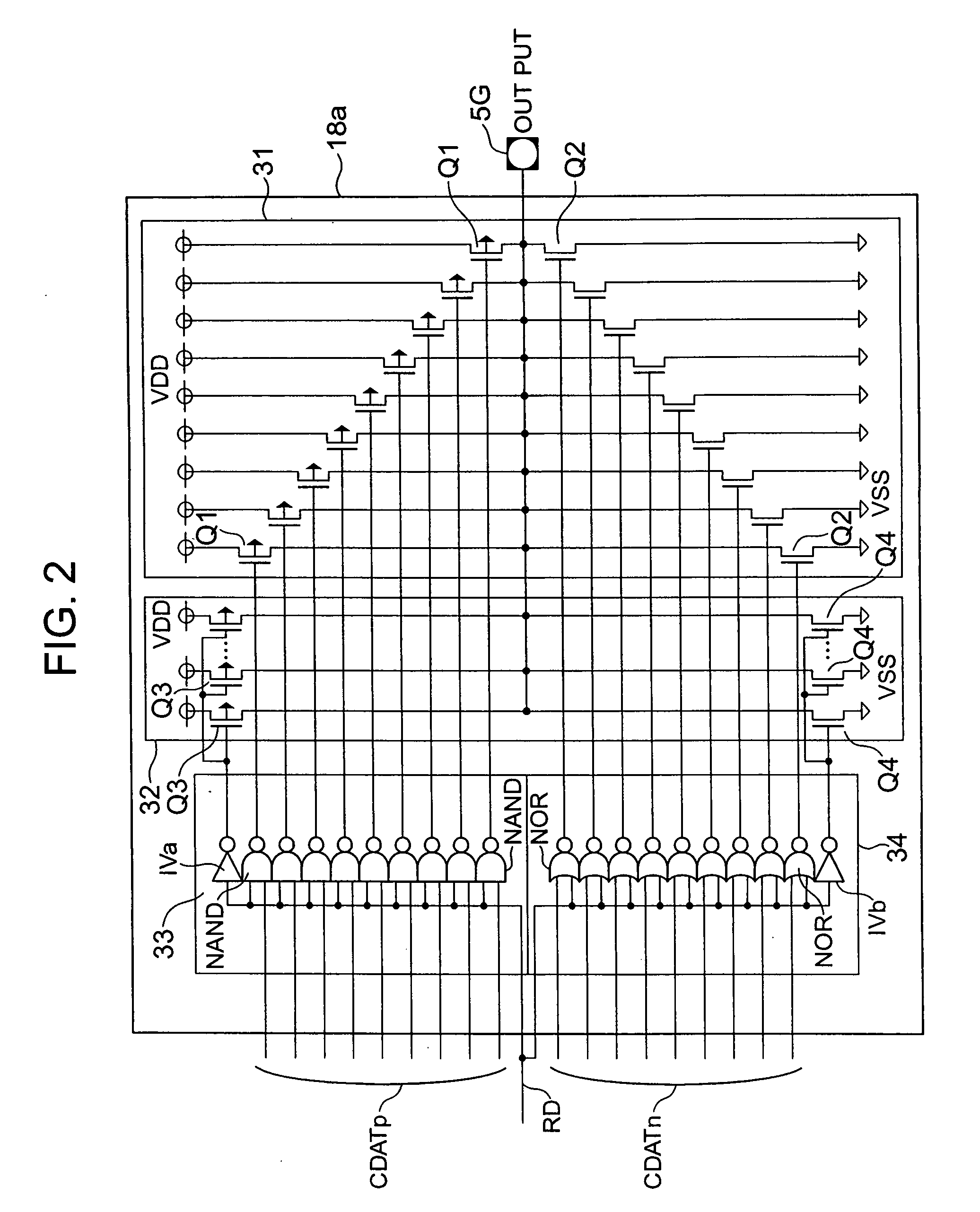
  • Figure 2
    Figure 2
  • Figure 3
    Figure 3
Patent Text Reader

Abstract

A semiconductor device is easy for high accuracy impedance matching against differences in impedance of a transmission line and a package wire. A semiconductor chip having external output buffers and a packaging circuit are included. Each external output buffer has a first output portion whose internal impedance is adjusted commonly with other external output buffers in accordance with impedance control data and a second output portion whose internal impedance is adjusted independently of other external output buffers. Both of the first and second output portions are connected in parallel to a common output terminal. Common adjustment by the first output portion can cope with impedance of the transmission line and individual adjustment by the second output portion can cope with a difference of package wires.
Need to check novelty before this filing date? Find Prior Art

Description

CROSS REFERENCE TO RELATED APPLICATIONS

[0001] This application is a Continuation application of U.S. application Ser. No. 10 / 983,723 filed on Nov. 9, 2004. Priority is claimed based on U.S. application Ser. No. 10 / 983,723 filed on Nov. 9, 2004, which claims priority to Japanese Patent Application No. 2003-385745 filed on Nov. 14, 2003, all of which is incorporated by reference.BACKGROUND OF THE INVENTION

[0002] This invention relates to a technology for regulating internal impedance of output buffers of a semiconductor device. For example, the invention relates to a technology that will be effective when applied to impedance matching of data output buffers in a semiconductor device such as an SRAM (Static Random Access Memory).

[0003] To reduce influences of signal reflection through a transmission line, it is necessary to highly accurately establish impedance matching that brings an internal impedance viewed from an external terminal of a semiconductor device into conformity with ...

Examples

Embodiment Construction

[0036]FIG. 1 mainly shows an impedance matching structure of an SRAM as an example of the semiconductor device according to the invention. The SRAM 1 shown in the Figure is fabricated on one semiconductor substrate such as a single crystal silicon substrate by a CMOS integrated circuit fabrication technology, or the like.

[0037] The SRAM 1 includes an SRAM chip 2 as a semiconductor chip (pellet) and a packaging circuit portion (hereinafter called also “package”) 3 combined with the SRAM 2, though the construction is not restrictive, in particular. The package 3 will be later described in detail but a construction for face-down package is hereby assumed. The SRAM chip 2 has a plurality of pad electrodes 5F, 5G to 5I typically shown as representatives of external terminals. The package 3 has a plurality of external connection terminals (packaging terminals) 6F, 6G to 6I typically shown as representatives of packaging terminals for packaging the SRAM 1 to a packaging substrate (not sho...