Impedance matching commonly and independently

a technology of impedance matching and common impedance, which is applied in the field of common impedance matching and independent impedance matching, can solve the problems of adjusting errors and operation that are difficult to control, and achieve the effect of improving impedance matching with the transmission line and high accuracy impedance matching

Active Publication Date: 2007-03-27
RENESAS ELECTRONICS CORP
View PDF4 Cites 15 Cited by
  • Summary
  • Abstract
  • Description
  • Claims
  • Application Information

AI Technical Summary

Benefits of technology

[0006]It is an object of the invention to provide a semiconductor device capable of easily establishing high accuracy impedance matching while a difference in impedance between a transmission line and package wires is taken into consideration.
[0009]As described above, common adjustment by the first output portion can cope with the impedance of the transmission line and individual adjustment by the second output portion can cope with the difference of the package wires. Therefore, highly accurate impedance matching can be easily achieved against the increase of the number of terminals of the external connection terminals and the unequal length of the package wires.
[0019]According to the invention, high accuracy impedance matching can be easily achieved while the difference in impedance between the transmission line and the package wire is taken into account and can improve impedance matching with the transmission line.

Problems solved by technology

To individually set the internal impedance of all the output buffers in this case, the internal impedances of all the output buffers must be individually adjusted while matching with the impedance of a transmission line and matching with the difference of the package wires are taken into consideration and this operation is very troublesome.
In addition, an adjusting error is likely to occur.

Method used


Image

  • Impedance matching commonly and independently
  • Impedance matching commonly and independently
  • Impedance matching commonly and independently

Examples


Embodiment Construction

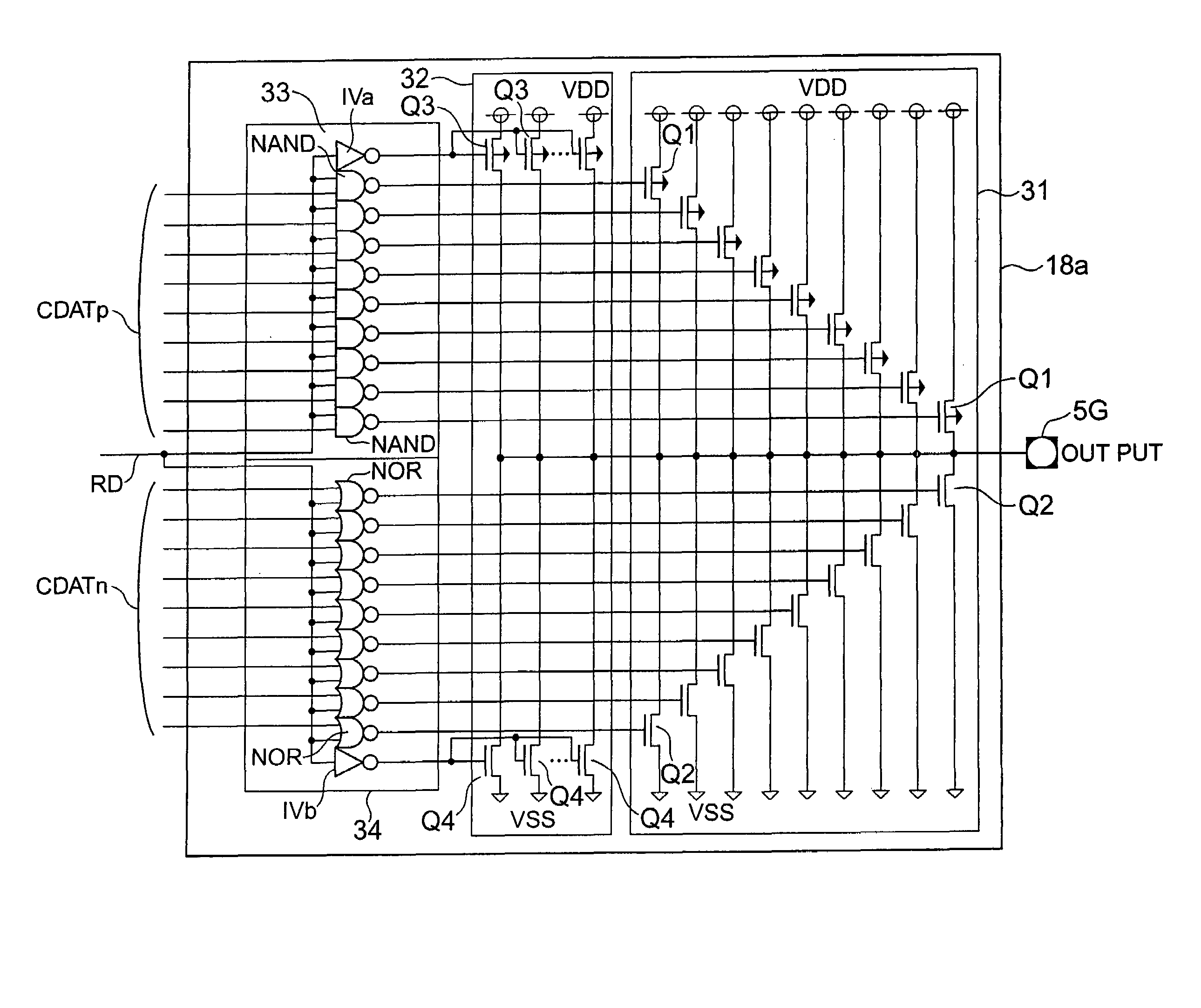
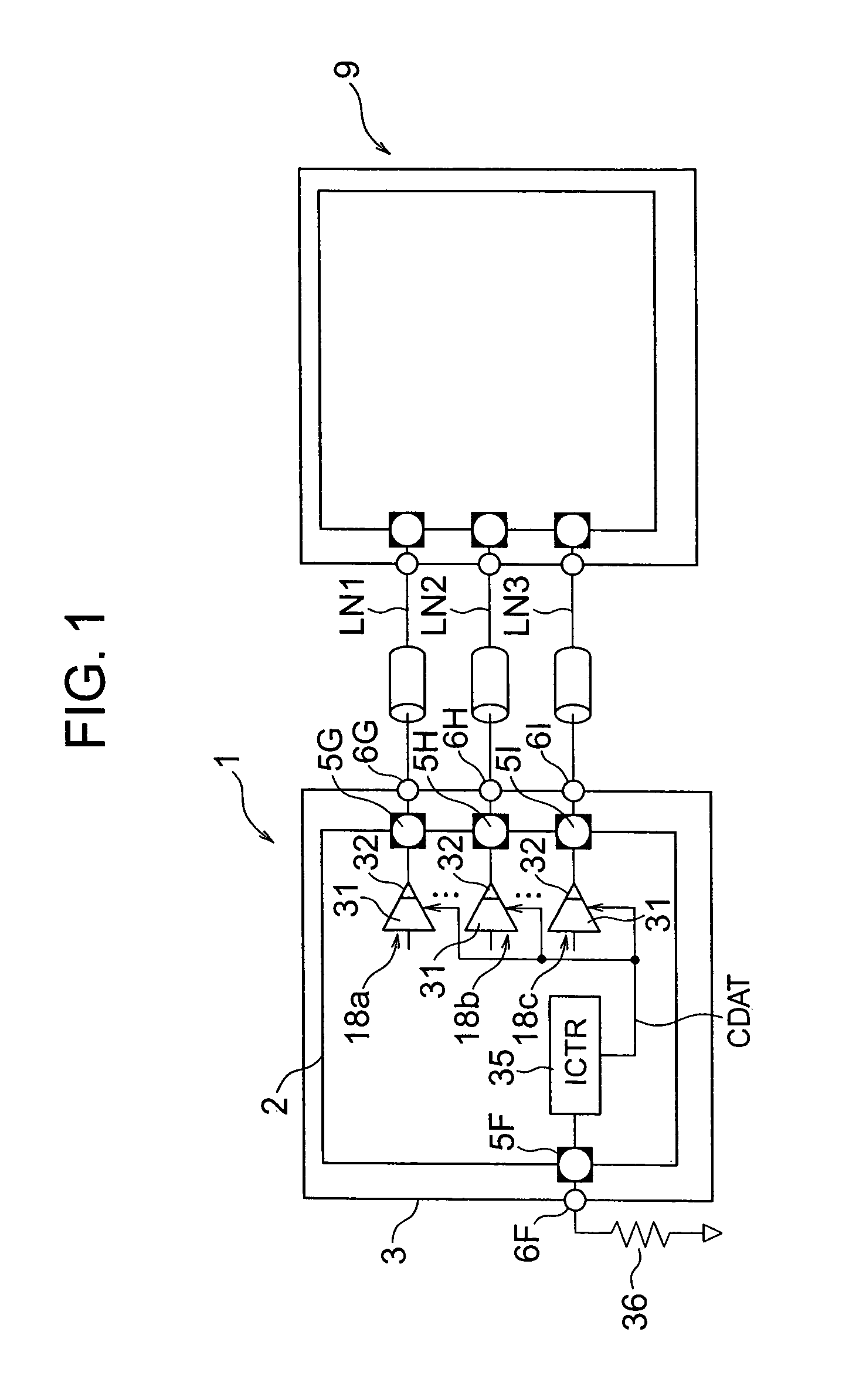
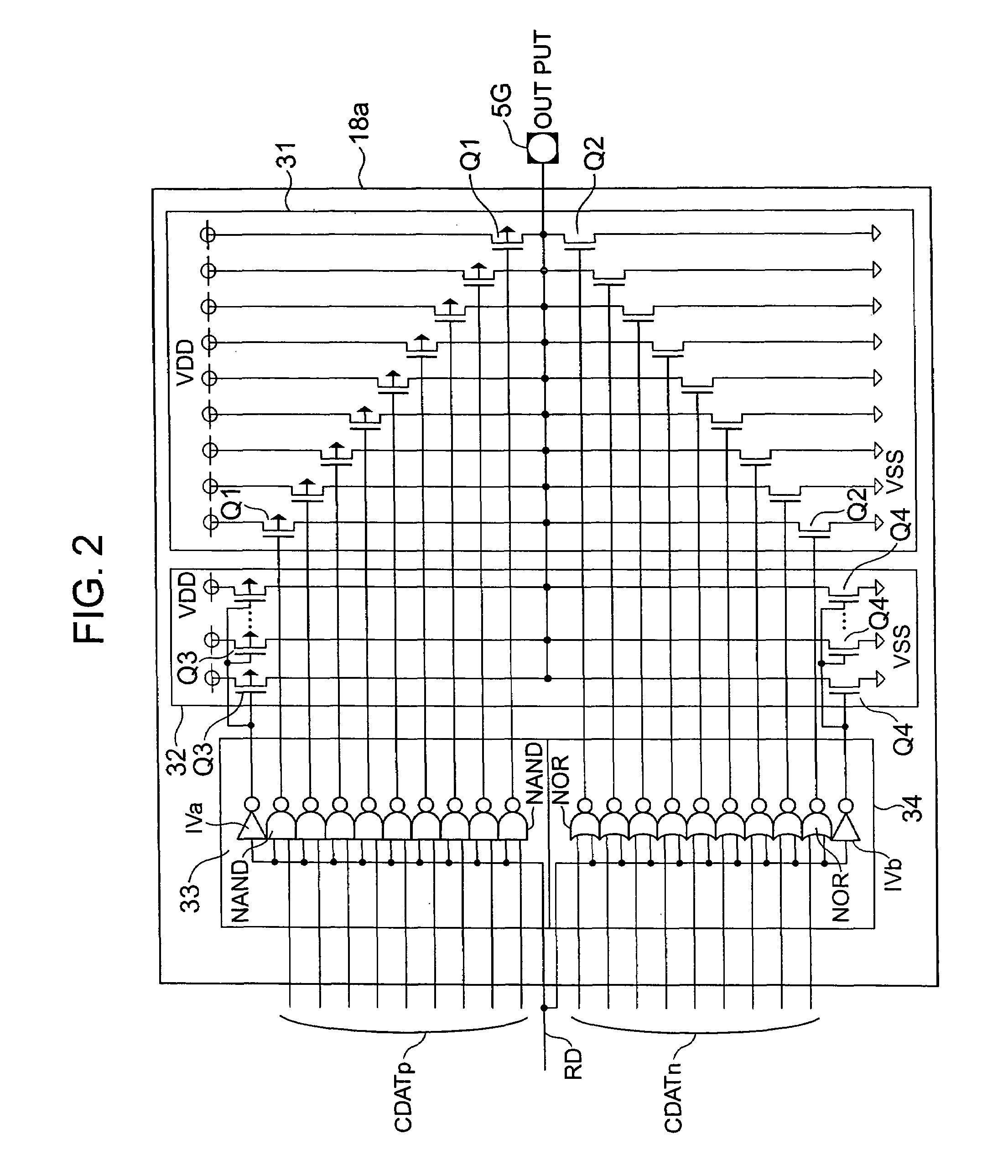
[0035]FIG. 1 mainly shows an impedance matching structure of an SRAM as an example of the semiconductor device according to the invention. The SRAM 1 shown in the Figure is fabricated on one semiconductor substrate such as a single crystal silicon substrate by a CMOS integrated circuit fabrication technology, or the like.

[0036]The SRAM 1 includes an SRAM chip 2 as a semiconductor chip (pellet) and a packaging circuit portion (hereinafter called also “package”) 3 combined with the SRAM 2, though the construction is not restrictive, in particular. The package 3 will be later described in detail but a construction for face-down package is hereby assumed. The SRAM chip 2 has a plurality of pad electrodes 5F, 5G to 5I typically shown as representatives of external terminals. The package 3 has a plurality of external connection terminals (packaging terminals) 6F, 6G to 6I typically shown as representatives of packaging terminals for packaging the SRAM 1 to a packaging substrate (not shown...


PUM


Abstract

A semiconductor device is easy for high accuracy impedance matching against differences in impedance of a transmission line and a package wire. A semiconductor chip having external output buffers and a packaging circuit are included. Each external output buffer has a first output portion whose internal impedance is adjusted commonly with other external output buffers in accordance with impedance control data and a second output portion whose internal impedance is adjusted independently of other external output buffers. Both of the first and second output portions are connected in parallel to a common output terminal. Common adjustment by the first output portion can cope with impedance of the transmission line and individual adjustment by the second output portion can cope with a difference of package wires.

Description

BACKGROUND OF THE INVENTION[0001]This invention relates to a technology for regulating internal impedance of output buffers of a semiconductor device. For example, the invention relates to a technology that will be effective when applied to impedance matching of data output buffers in a semiconductor device such as an SRAM (Static Random Access Memory).[0002]To reduce influences of signal reflection through a transmission line, it is necessary to highly accurately establish impedance matching that brings an internal impedance viewed from an external terminal of a semiconductor device into conformity with the impedance of a transmission line.[0003]Because the internal impedance changes in accordance with driving capacity of output buffers, JP-A-05-166931, (especially in FIGS. 1–3) describes a circuit construction in which a plurality of clamp resistors are connected in parallel on the side of a ground potential of a push-pull output circuit and are taken out to pad electrodes of a se...

Claims


Application Information

Patent Timeline
Patent Type & Authority Patents(United States)
IPC IPC(8): H03K19/003G11C11/417H01L21/822H01L23/12H01L27/04H03K19/00H03K19/0175H04L25/02
CPCH03K19/0005H04L25/0278H04L25/0272H04L25/028H01L2924/30107H01L2224/49175H01L2224/48137H01L2924/13091H01L2924/3011H01L2924/00H01L2224/05554H01L2924/00014H01L2924/30111H01L2224/45099
Inventor UENO, HIROKI
Owner RENESAS ELECTRONICS CORP
Why Eureka
Try Eureka